¶ W25Q128JV SPI Flash memory module
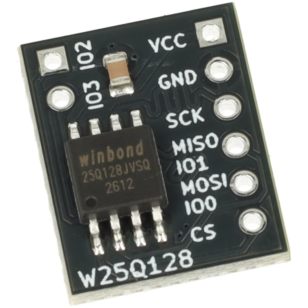
In brief: The W25Q128JV module provides 128 Mbit (16 MiB) of non-volatile storage for a microcontroller through SPI, Dual SPI or Quad SPI.
Important: The module requires a 3,3 V supply and matching logic levels. It has no voltage regulator or logic-level converters.
| Information | Value |
|---|---|
| Product name | W25Q128JV SPI Flash memory module |
| Integrated circuit | Winbond W25Q128JVSIQ |
| Module manufacturer | embidi |
| Memory type | Non-volatile SPI NOR Flash |
| Capacity | 128 Mbit = 16 MiB = 16,777,216 bytes |
| Interface | SPI / Dual SPI / Quad SPI |
| Power supply | 3,3 V nominal, 2,7–3,6 V operating range |
| Logic levels | Referenced to VCC; no 5 V level conversion |
| CS pull-up resistor | Not fitted on the module |
| Last updated | 2026-11-06 |
¶ Description
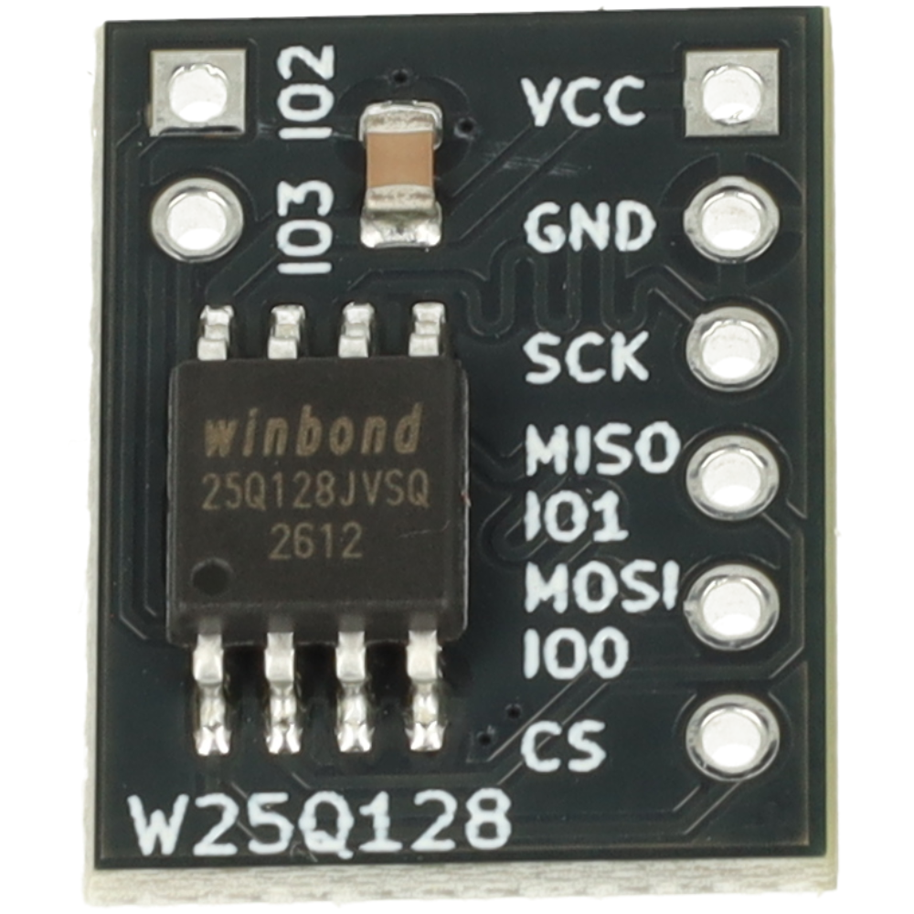
The module brings the W25Q128JVSIQ memory signals out to two pin headers. J2 provides power and the four signals used for standard SPI. J1 provides IO2 and IO3 for Quad SPI. All eight connections are labelled on the top side of the PCB.
The board contains the memory IC and a supply decoupling capacitor. VCC connects directly to the memory supply. The module has no voltage regulator, logic-level converters or onboard pull-up resistors.
¶ Module views
| Top view | Bottom view | Module and pin header |
|---|---|---|
 |
 |
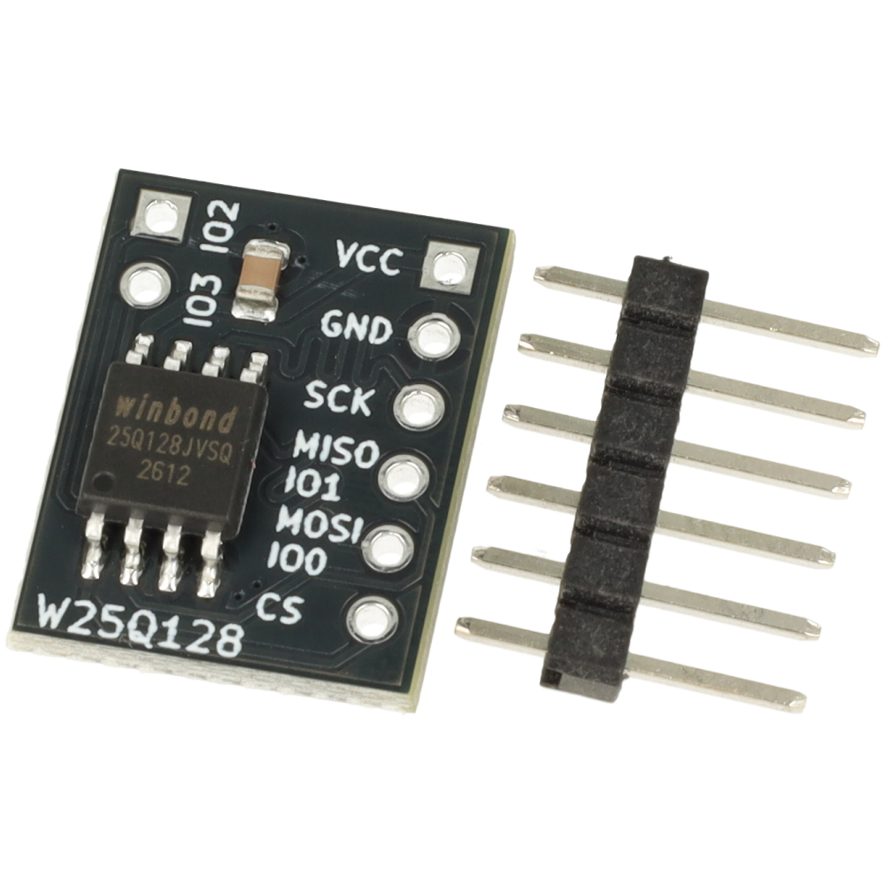 |
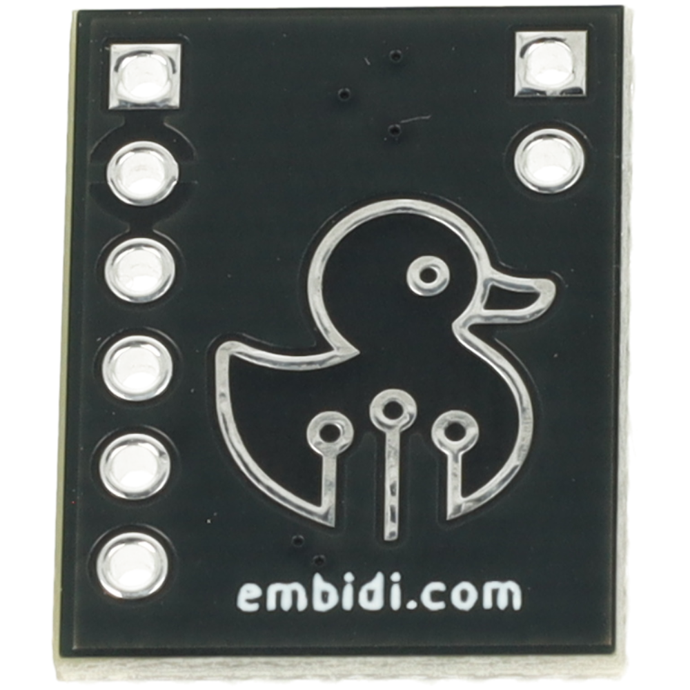
The photographs show the module before the pin header is soldered.
¶ Key features
- W25Q128JVSIQ non-volatile NOR Flash memory,
- 128 Mbit (16 MiB) capacity,
- SPI, Dual SPI and Quad SPI interfaces,
- 3,3 V supply and logic levels,
- all memory signals accessible on 2,54 mm headers,
- separate IO2 and IO3 connections for Quad SPI,
- compact two-layer PCB with supply decoupling.
¶ Typical applications
- storing measurement logs and configuration data,
- keeping graphics, fonts, audio samples and other application resources outside the microcontroller,
- prototyping external-memory drivers and testing SPI or QSPI peripherals.
The application controls the storage layout. A filesystem or wear-levelling layer must be provided by the software when needed.
¶ Specifications
| Parameter | Value | Notes |
|---|---|---|
| Integrated circuit | W25Q128JVSIQ | SOIC-8, 208 mil |
| Capacity | 16 MiB | 128 Mbit |
| Supply voltage | 2,7–3,6 V | Use a regulated 3,3 V supply |
| Interfaces | SPI, Dual SPI, Quad SPI | Selected by commands and host configuration |
| Maximum IC clock | Up to 133 MHz | Command-dependent IC rating; wiring and the host limit the usable module clock |
| SPI modes | Mode 0 or Mode 3 | MSB first |
| Program page | 256 bytes | Split writes at page boundaries |
| Erase sizes | 4 KiB / 32 KiB / 64 KiB / entire chip | Erasing removes the previous contents |
| IC temperature range | −40 to +85 °C | W25Q128JVSIQ grade |
| Main connector | J2, 1×6 pins | 2,54 mm pitch |
| Additional data connector | J1, 1×2 pins | 2,54 mm pitch |
| PCB dimensions | 13,45 × 17,175 mm | Board outline, excluding headers |
| PCB thickness | 1,6 mm | Two-layer PCB |
IC ratings are described in the W25Q128JV datasheet.
¶ Pinout
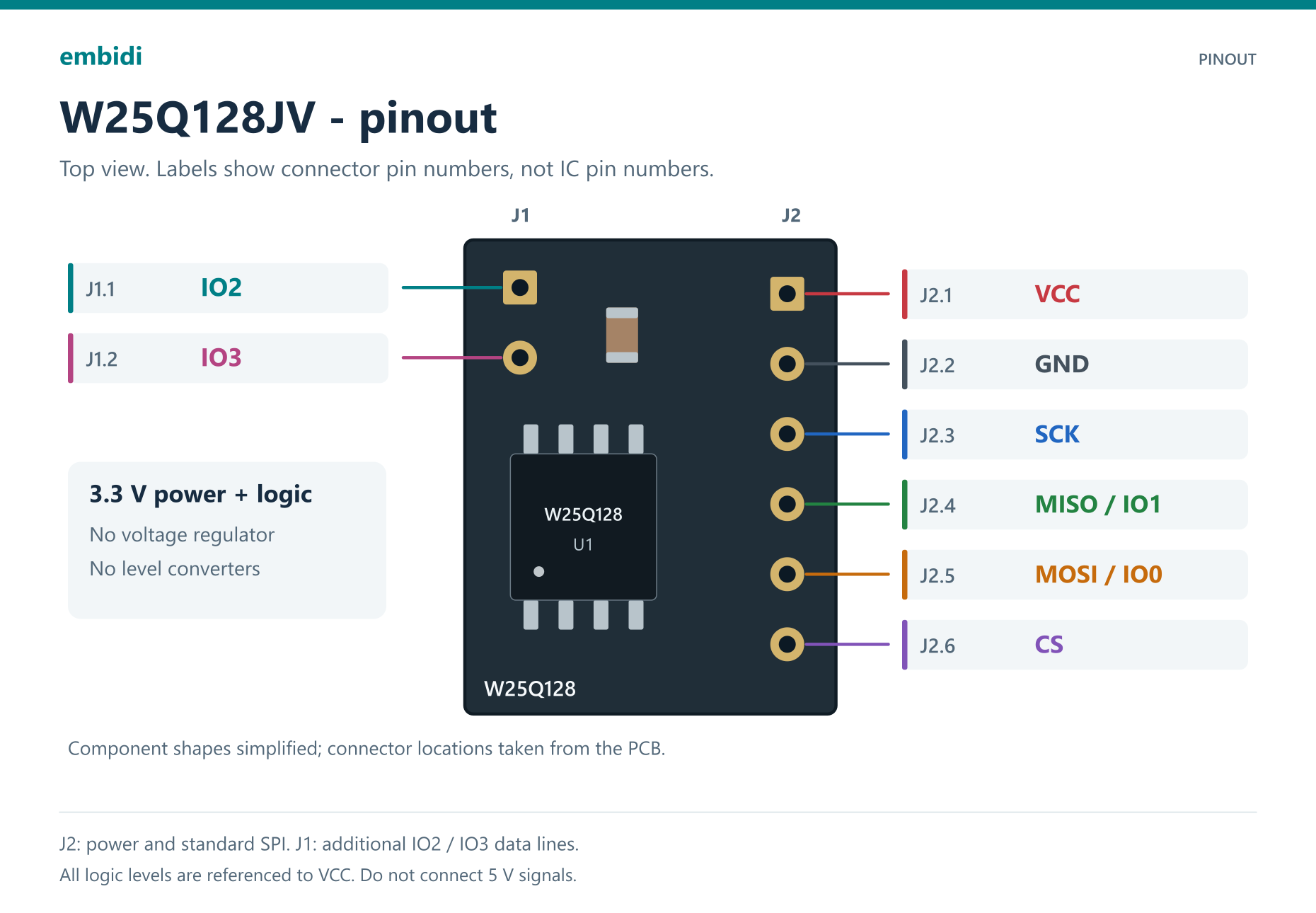
Viewed from the top side, with the W25Q128 marking at the bottom, J2 is on the right and J1 is at the upper left. Header pin numbers below are the project connector numbers, not the IC pin numbers. Directions are relative to the memory module.
¶ J2 — power and SPI
A 1×6 pin header with a 2,54 mm pitch. Signal names are marked on the top side of the board. Directions in the table apply to standard SPI and are given relative to the module.
| Pin | Signal | Type | Direction | Level | Description |
|---|---|---|---|---|---|
| 1 | VCC | Power | Input | 3,3 V nominal | Memory supply |
| 2 | GND | Power | — | 0 V | Common power and signal ground |
| 3 | SCK | Digital | Input | VCC logic | Clock from the microcontroller |
| 4 | MISO / IO1 | Digital | Output | VCC logic | Data to the microcontroller; IO1 in Dual/Quad SPI |
| 5 | MOSI / IO0 | Digital | Input | VCC logic | Data from the microcontroller; IO0 in Dual/Quad SPI |
| 6 | CS | Digital | Input | VCC logic | Chip select, active low |
In Dual and Quad transfers, IO0 and IO1 change direction according to the selected command.
¶ J1 — additional Quad SPI signals
A 1×2 pin header with a 2,54 mm pitch. The two additional data lines are used for Quad SPI transfers.
| Pin | Signal | Type | Direction | Level | Description |
|---|---|---|---|---|---|
| 1 | IO2 | Digital | Bidirectional | VCC logic | Third data line; connected to IC pin 3 |
| 2 | IO3 | Digital | Bidirectional | VCC logic | Fourth data line; connected to IC pin 7 |
With the module oriented as shown, IO2 is above IO3. In the schematic, these IC pins use the generic names /WP and /HOLD. For the fitted W25Q128JVSIQ, Quad Enable is factory fixed to 1 and /HOLD is disabled. Standard SPI does not use J1. See datasheet sections 7.1.4 and 11 for variant details.
¶ Connection
¶ Standard SPI
Connect VCC to a regulated 3,3 V supply, join the grounds, and connect SCK, MISO, MOSI and CS to the host. Keep the wires short and begin with a low clock, such as 1 MHz.
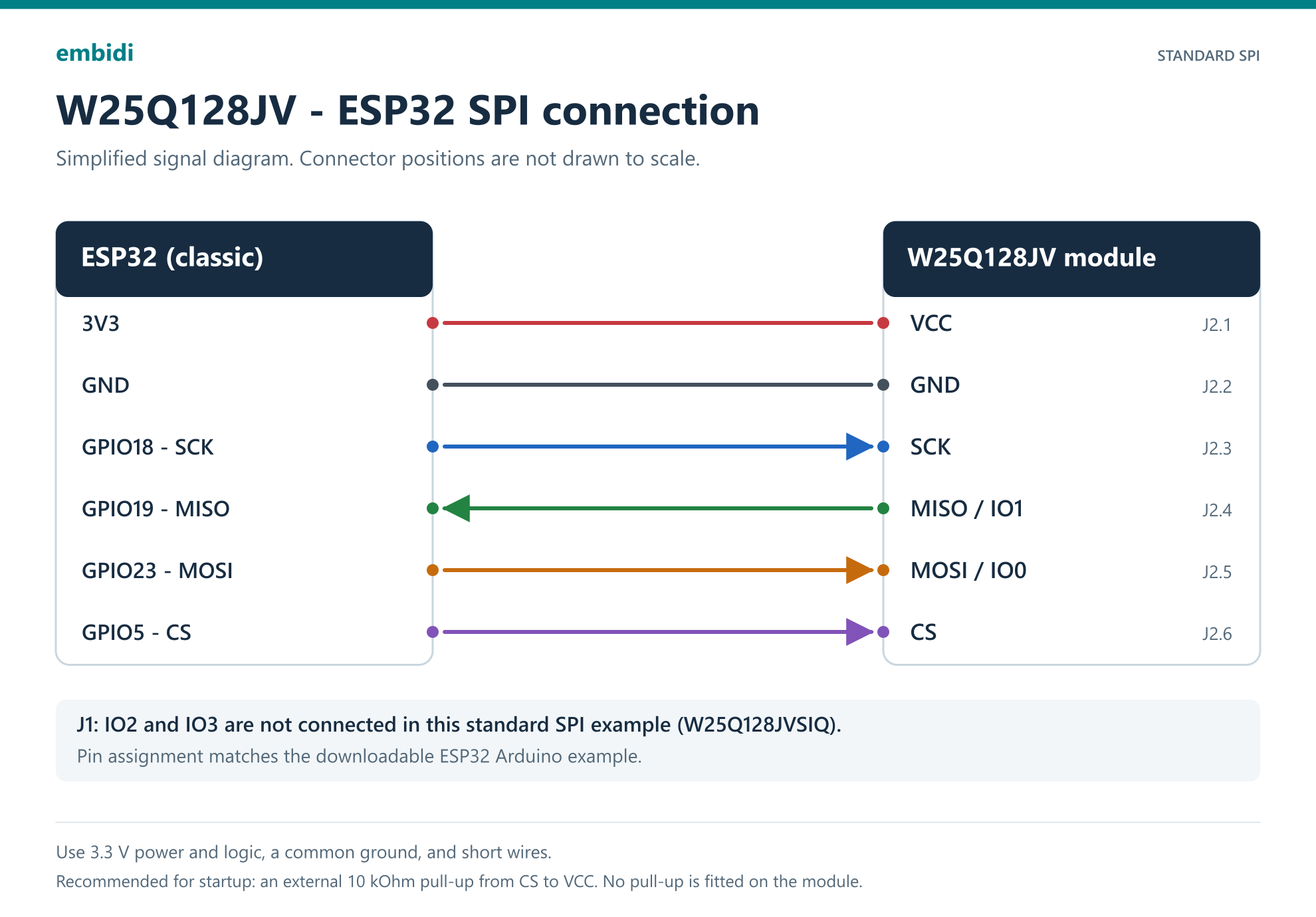
Keep CS high when the memory is not selected. An external pull-up, for example 10 kΩ from CS to VCC, helps keep it deselected while the host resets. The board has no CS pull-up.
¶ Example connections to popular platforms
The following table applies to the downloadable examples, using standard SPI and 3,3 V logic.
| Signal | Module pin | ESP32 example | STM32G474 SPI example | Notes |
|---|---|---|---|---|
| Supply | J2.1 / VCC | 3V3 | 3,3 V supply | Regulated 3,3 V source |
| Ground | J2.2 / GND | GND | GND | Common ground |
| Clock | J2.3 / SCK | GPIO18 | PA5 / SPI1_SCK | Host output to the memory |
| Receive | J2.4 / MISO / IO1 | GPIO19 | PA6 / SPI1_MISO | Memory output to the host |
| Transmit | J2.5 / MOSI / IO0 | GPIO23 | PA7 / SPI1_MOSI | Host output to the memory |
| Chip select | J2.6 / CS | GPIO5 | PB6 / SPI1_CS | Active low; keep high when not selected |
| Additional data | J1.1 / IO2 | Unconnected | Unconnected | Not used by the standard SPI examples |
| Additional data | J1.2 / IO3 | Unconnected | Unconnected | Not used by the standard SPI examples |
The pin assignments above match the downloadable example projects. The ESP32 example uses the VSPI bus, while the STM32G474 example uses SPI1. When adapting a project to another board, update its GPIO and peripheral configuration to match the wiring.
¶ Quad SPI
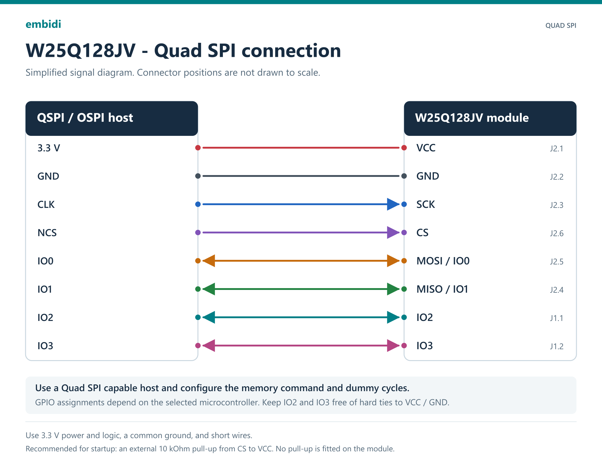
Connect SCK, CS and all four data lines, IO0–IO3, to a compatible host peripheral. Use the host's QSPI/OSPI driver with the appropriate command, address and dummy-cycle settings. Exposing IO2 and IO3 does not make an ordinary four-wire SPI driver perform Quad transfers. Leave these lines free of hard connections to VCC or GND when using Quad SPI.
¶ Important information and limitations
- Supply VCC from a regulated 3,3 V source and connect a common ground with the microcontroller.
- VCC and the signal pins connect directly to the memory IC. A host using 5 V logic requires suitable level conversion.
- Keep CS high when the memory is not selected. The module has no onboard CS pull-up.
- Use short connections and select an SPI clock appropriate for the wiring and the host.
- Quad SPI requires a compatible host peripheral, all four data lines and the correct command configuration.
- Programming and erasing must be handled by the driver. Preserve data that must survive an erase and split writes at page boundaries.
¶ Software
The W25Q128JV is controlled through the microcontroller's SPI peripheral. The software configures the interface and handles memory commands, programming and erasing. Ready-to-use examples are available for the following platforms.
| Platform | Interface | Example |
|---|---|---|
| ESP32 | SPI | Downloadable ESP32 project |
| STM32G474 | SPI | Downloadable STM32G474 project |
The GPIO assignment and SPI configuration must match the selected example project.
Important: Both supplied examples erase and rewrite the 4 KiB sector starting at address
0x000000. Save any contents you need before running them.
¶ ESP32 example
A ready-to-use Arduino sketch is available for ESP32. The example erases a sector, writes a test string and reads it back. Results are printed to the serial monitor at 115200 baud. Connections are listed in the table above.
Download the ESP32 example for W25Q128
¶ STM32G474 example
A ready-to-use STM32CubeIDE project is available for STM32G474. The archive includes the CubeMX .ioc configuration and a W25Q128 driver. The example uses SPI1, reads the JEDEC ID, then erases, writes and reads test data.
Download the STM32G474 SPI example for W25Q128
¶ Troubleshooting
| Symptom | Checks |
|---|---|
ID reads FF FF FF or 00 00 00 |
Check VCC at the module, common GND, CS and the MISO/MOSI connections. These values alone do not identify the fault. |
| Communication is intermittent | Shorten wires, check ground connections and lower the SPI clock. |
| Standard SPI works but Quad SPI does not | Check IO2/IO3 wiring and the host's command and dummy-cycle configuration. |
| Reads work but programming fails | Check software protection, erase state, Write Enable and BUSY handling. |
¶ Files
| File | Format | Version | Description |
|---|---|---|---|
| W25Q128JV datasheet | March 2018 (Rev. F) | Winbond W25Q128JV datasheet | |
| Module schematic | 2026-10-27 | Electrical schematic | |
| Dimension drawing | 2026-10-27 | PCB dimensions | |
| 3D model | STEP | 2026-10-27 | 3D model |