¶ L6983 5 V Step-Down Converter Module
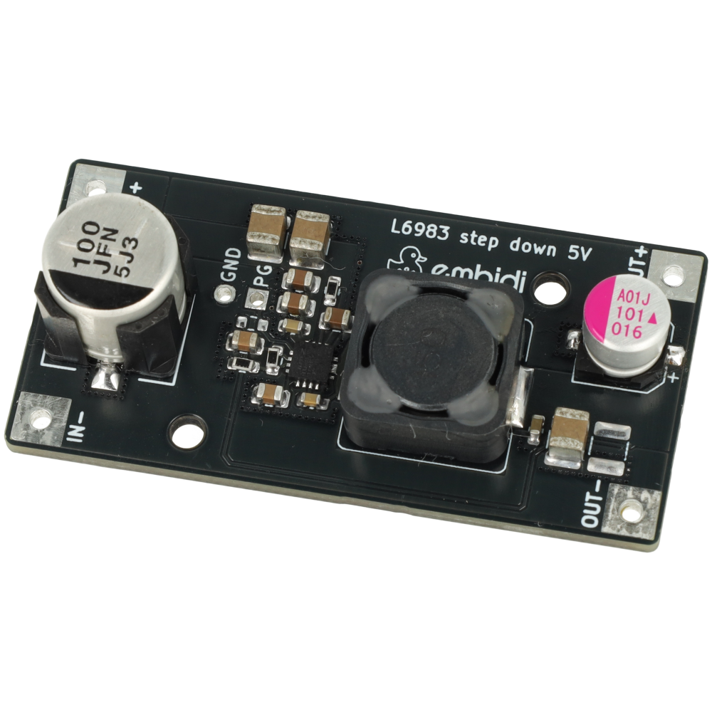
In short: The L6983 module converts a higher DC supply voltage into a nominal 5 V output for powering electronic circuits and development boards.
Important: This is a step-down converter with a fixed 5 V output. Use the marked IN+ / IN− and OUT+ / OUT− connections and check that the connected device accepts a 5 V supply.
| Information | Value |
|---|---|
| Product name | L6983 5 V Step-Down Converter Module |
| Integrated circuit | STMicroelectronics L6983NQTR |
| Module manufacturer | embidi |
| Module type | Synchronous step-down DC/DC converter |
| Tested input range | 6–31 V DC |
| Output voltage | 5 V nominal |
| Tested output current | 2.5 A; see measurement conditions below |
| Last update | 2026-11-16 |
¶ Description
The module provides a nominal 5 V supply from a higher DC voltage. It can be used to power 5 V electronics from 12 V or 24 V supplies, or from another DC source within the tested input range.
The converter starts automatically when input power is applied. The output voltage is fixed, so no adjustment or software configuration is required. Input and output share a common ground. An optional power-good signal indicates when the output is valid.
¶ Module views
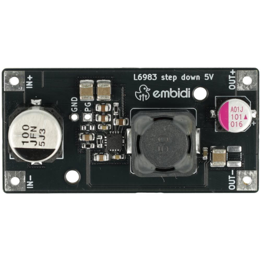
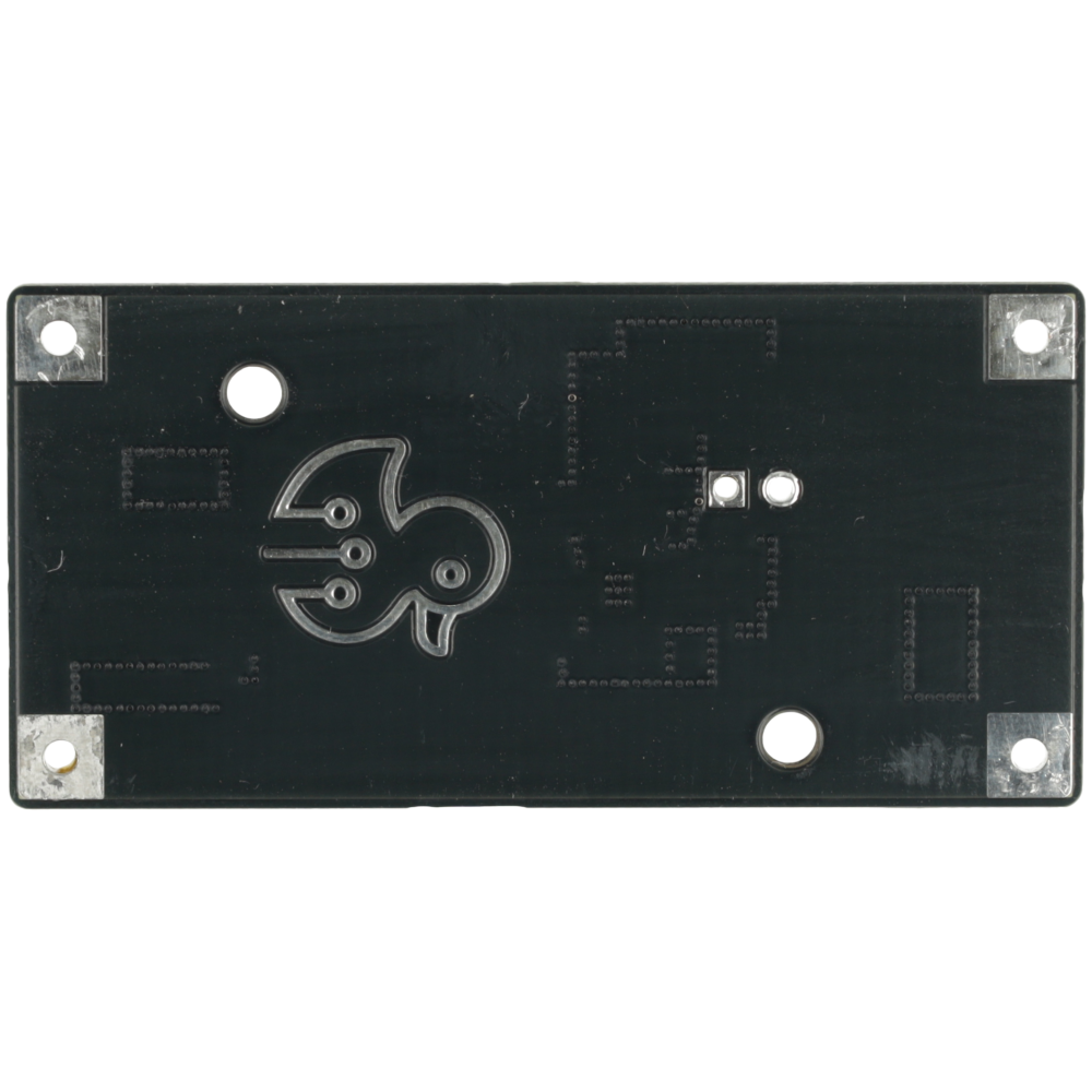
| Top view | Bottom view |
|---|---|
¶ Key features
- nominal 5 V output,
- tested at 6 V, 12 V, 24 V and 31 V input,
- 2.5 A output tested under the conditions listed below,
- low-noise operation and low measured output ripple,
- automatic startup,
- optional power-good signal,
- clearly marked input and output connections,
- two mounting holes.
¶ Typical applications
- supplying 5 V development boards and controllers,
- powering sensors, displays and peripheral modules that accept 5 V,
- converting a 12 V or 24 V DC supply to 5 V,
- embedded-system prototypes.
¶ Specifications
| Parameter | Value | Notes |
|---|---|---|
| Integrated circuit | L6983NQTR | STMicroelectronics |
| Converter type | Synchronous buck | Non-isolated, common ground |
| Tested input range | 6–31 V DC | Tested at 6 V, 12 V, 24 V and 31 V |
| Output voltage | 5 V nominal | Fixed output; no adjustment required |
| Tested output current | 2.5 A | 24 °C ambient, no forced airflow; tests lasting 20 minutes |
| Peak measured efficiency | Approximately 95.2% at 12 V; 93.2% at 24 V | At 0.5 A and 1 A output respectively; see measurements |
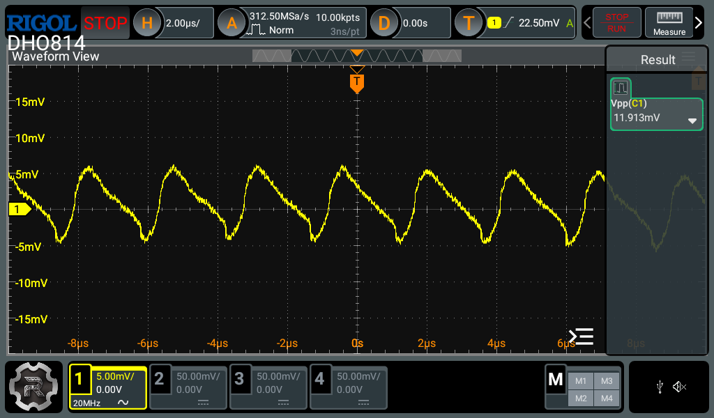
| Measured output ripple | Approximately 11.9 mVpp | 24 V input, 2.5 A output, 20 MHz measurement bandwidth |
| No-load input current | Approximately 6.1 mA at 12 V; 5.7 mA at 24 V | Measured on the module |
| Switching frequency | 400 kHz nominal | Low-noise operating mode |
| Power-good output | Open collector with pull-up to VOUT | High level approaches 5 V; optional connection |
| Startup | Automatic | Starts when input voltage is applied |
| PCB dimensions | 50.29 × 24.65 mm | Board dimensions |
| PCB thickness | 1.60 mm nominal | Excludes components |
| Mounting holes | 2 × Ø2.5 mm | Corner power-connection holes are not mounting holes |
The measured electrical and thermal results describe the stated test conditions. Check cooling and temperature in the intended enclosure and operating environment.
¶ Pinout
| Pin / pad | Type | Direction | Level | Description |
|---|---|---|---|---|
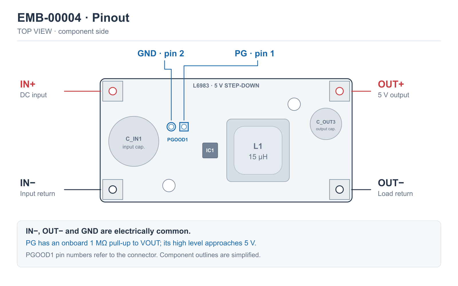
| IN+ | Power | Input | 6–31 V DC tested | Positive supply input |
| IN− | Power | — | 0 V | Input ground |
| OUT+ | Power | Output | 5 V nominal | Positive output to the load |
| OUT− | Power | — | 0 V | Load return |
| PG | Digital | Output | 0 V / VOUT | Optional power-good signal |
| GND | Power | — | 0 V | Power-good signal ground |
In the component-side top view, IN+ / IN− are on the left and OUT+ / OUT− on the right. The small PG connection is the right-hand square pad, pin 1; its GND is the left-hand round pad, pin 2. IN−, OUT− and GND are electrically common.
¶ Connection
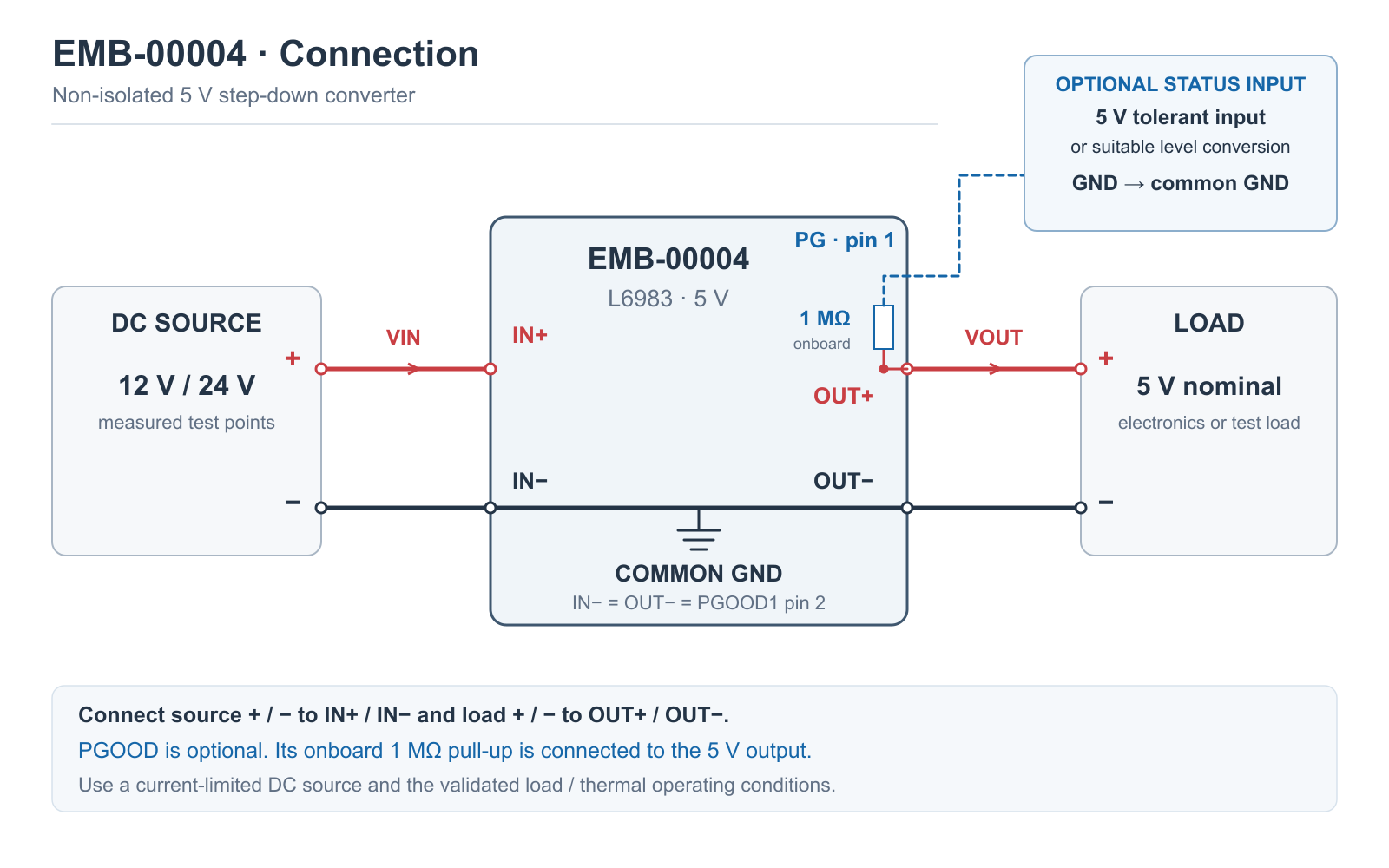
| Source / load | Module connection |
|---|---|
| DC source positive | IN+ |
| DC source negative | IN− |
| 5 V load positive | OUT+ |
| Load ground | OUT− |
| Optional compatible status input | PG |
| Status-input ground | GND |
- With power off, connect the DC source to IN+ / IN− and check polarity.
- Connect the 5 V load to OUT+ / OUT−.
- Apply input power. The converter starts automatically.
- Verify approximately 5 V at the output before using the module with sensitive electronics.
Use a current-limited supply for initial setup. Keep power leads short and suitable for the load current; voltage drop in the leads reduces the voltage reaching the connected device.
¶ Power-good output
PG indicates that the output voltage is valid. The connection is optional and may be left unconnected when it is not needed.
PG is pulled up to the 5 V output through 1 MΩ. Connect it to a 5 V-tolerant input or use suitable level conversion. The weak pull-up means that input leakage and probe loading can affect the observed high level and rise time. Do not treat PG as a push-pull output.
¶ Important information and limitations
- The output is fixed at 5 V. Do not connect it directly to a device that accepts only 3.3 V.
- Observe input polarity. The module has no onboard reverse-polarity protection, input fuse or TVS.
- Input and output are not galvanically isolated; all ground connections are common.
- Provide cooling appropriate to the load and ambient temperature, especially inside an enclosure.
- Use the two Ø2.5 mm mounting holes. The corner holes are electrical power connections.
- Do not connect OUT+ to another active supply or parallel modules without a suitable arrangement.
¶ Measurements
The results below show measurements made on the module. Thermal tests used a 2.5 A load, 24 °C ambient temperature and no forced airflow. Each thermal test lasted 20 minutes.
¶ Output voltage and efficiency
| Output current [A] | VOUT at 12 V input [V] | Efficiency at 12 V [%] | VOUT at 24 V input [V] | Efficiency at 24 V [%] |
|---|---|---|---|---|
| 0 | 5.00 | — | 5.00 | — |
| 0.1 | 5.00 | 85.7 | 5.00 | 76.4 |
| 0.5 | 4.99 | 95.2 | 4.99 | 92.0 |
| 1 | 4.99 | 95.1 | 4.99 | 93.2 |
| 2 | 4.98 | 92.9 | 4.97 | 91.8 |
| 2.5 | 4.97 | 91.4 | 4.97 | 90.5 |
| 3 | 4.96 | 89.6 | 4.96 | 88.9 |
The input voltages above are nominal settings. Efficiencies are approximate measured results for this setup.
At the 0.1 A point, the measured output current was 0.100 A with 12 V input and 0.101 A with 24 V input.
The 3 A row is a DC measurement point. The thermal tests below were performed at 2.5 A.
¶ Output ripple
| Input voltage | Output current | Measured ripple |
|---|---|---|
| 24 V | No external load | Approximately 10.5 mVpp |
| 24 V | 2.5 A | Approximately 11.9 mVpp |
The waveform below shows the output ripple at 24 V input and 2.5 A load. Measurement bandwidth was limited to 20 MHz. The indicated ripple includes probe and instrument noise.
¶ Startup and power-good
The waveform below shows startup with a 1 A load and a supply set to 24 V. Yellow: VOUT; cyan: PG. The input voltage was ramped up by the bench supply, so this capture illustrates the complete supply-start sequence.
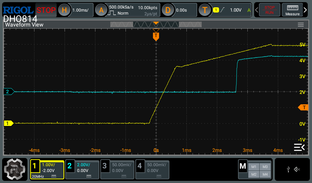
PG changes state as the output reaches its valid voltage. Its weak pull-up means that a passive oscilloscope probe can reduce the observed PG high level.
¶ Load switching
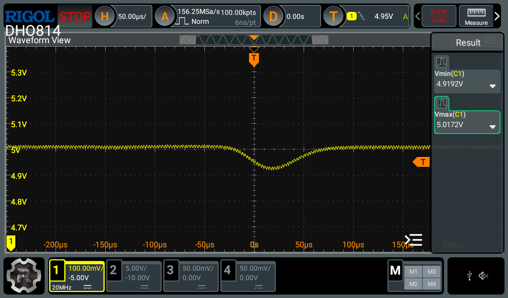
The captures below show the output response when the electronic load was manually switched between off and a 2.5 A setting, with the 24 V input left on.
| Electronic-load setting change | Minimum recorded VOUT [V] | Maximum recorded VOUT [V] |
|---|---|---|
| Off → 2.5 A | 4.919 | 5.017 |
| 2.5 A → Off | 4.915 | 5.020 |
Load applied:
Load removed:
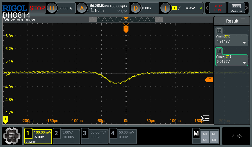
These are examples of manual electronic-load switching. The actual current transition rate was not measured; the displayed voltage excursions describe this test setup.
¶ Temperature under load
| Input voltage [V] | IC case temperature [°C] | Operating time [min] |
|---|---|---|
| 6 | 77 | 20 |
| 12 | 72 | 20 |
| 24 | 75 | 20 |
| 31 | 82 | 20 |
All four tests used a 2.5 A load, 24 °C ambient and natural convection without forced airflow. Temperatures were measured on the IC package surface. Allow air circulation around the module and check temperature in the intended enclosure; these finite-duration tests do not characterize every ambient or cooling condition.
Startup with the 2.5 A load already connected was also checked at 6 V and 31 V. The module started correctly at both endpoints and the corrected output voltage was 5.00 V in each case. The upper test point was limited by the available bench supply.
¶ Troubleshooting
| Symptom | What to check |
|---|---|
| No output voltage | Input polarity, voltage at IN+ / IN−, supply current limit and wiring |
| Voltage at the load is too low | Load current, power-lead length and thickness, connector resistance and source voltage |
| Repeated startup or shutdown | Supply current limiting, input-voltage drop, excessive load or overheating |
| PG level is lower than expected | Receiving-input leakage, oscilloscope probe loading and compatibility with the weak pull-up |
¶ Mechanical dimensions
The PCB measures 50.29 × 24.65 mm, with a nominal thickness of 1.60 mm and two Ø2.5 mm mounting holes. The four corner holes are power connections.
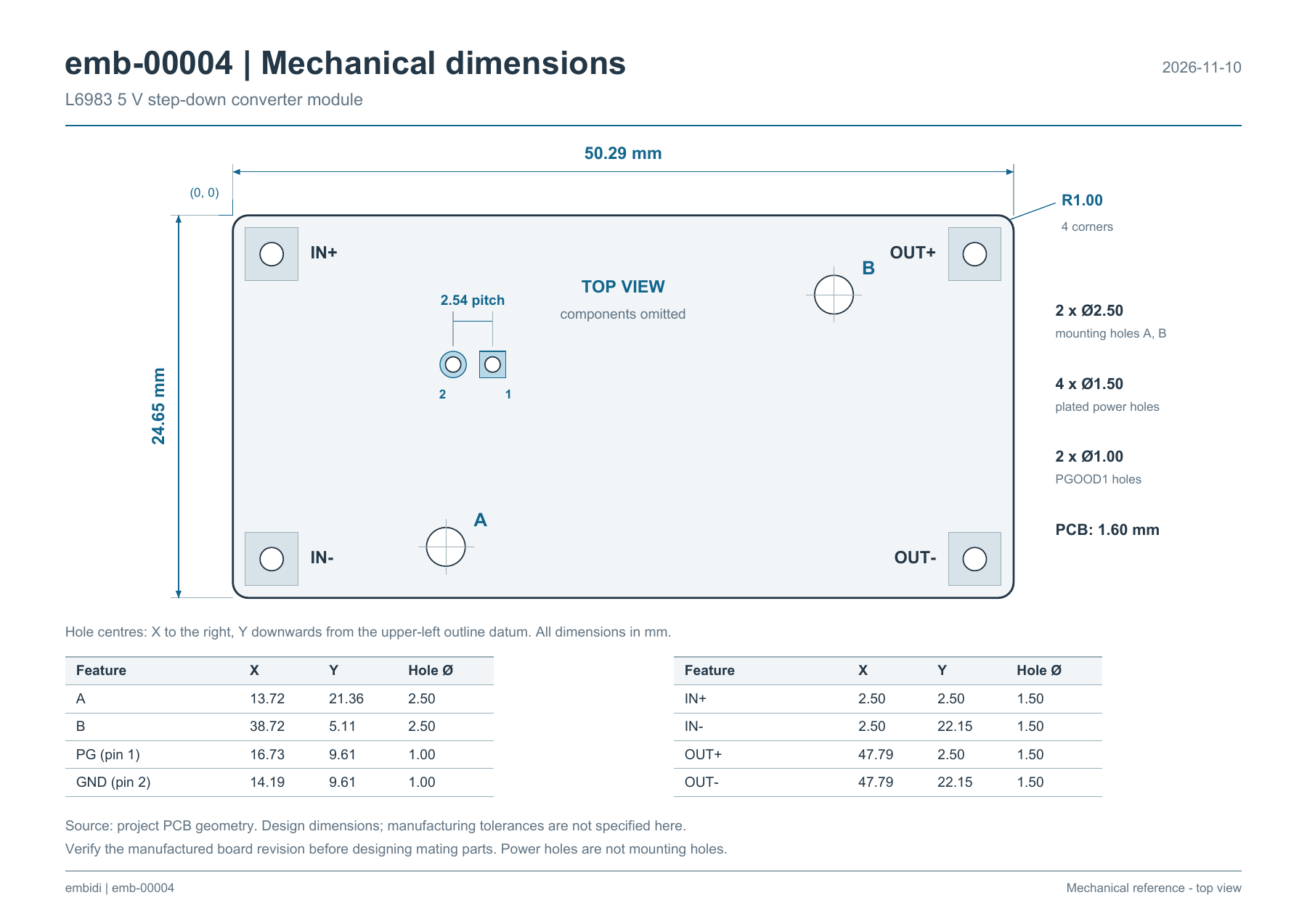
A dimension drawing (PDF) and STEP model are available for mechanical integration. The STEP uses simplified maximum component envelopes; see the model notes when planning enclosure clearances.
¶ Files
| File | Format | Version | Description |
|---|---|---|---|
| L6983 datasheet | DS13116 Rev. 4 | STMicroelectronics IC datasheet | |
| Module schematic | 2026-11-10 | Electrical schematic | |
| Dimension drawing | 2026-11-10 | PCB dimensions and mounting holes | |
| 3D model | STEP | 2026-11-10 | Mechanical model with simplified component envelopes |
| 3D model notes | TXT | 2026-11-10 | Model dimensions and enclosure-clearance notes |