¶ ADS1115 16-bit 4-channel ADC module
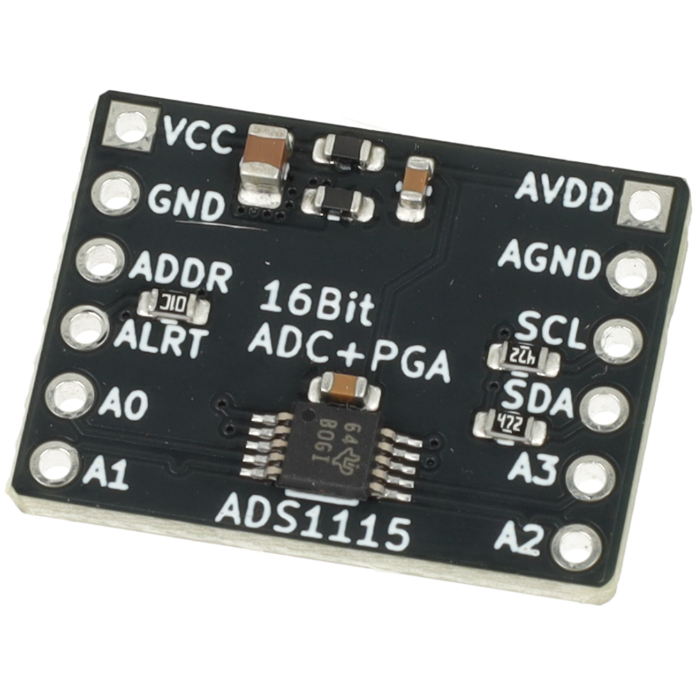
In brief: The ADS1115 module adds four single-ended analog inputs or differential voltage measurements to a microcontroller over I²C. It includes a programmable gain amplifier, an internal reference and oscillator, and filtering of the ADC supply and ground.
Important: SDA, SCL and ALRT have onboard pull-ups to VCC. For the supplied ESP32 and STM32 examples, power VCC/GND from 3.3 V and connect ADDR to GND for address 0x48. Every analog input must remain between AGND and AVDD, regardless of the selected full-scale range.
| Information | Value |
|---|---|
| Product name | ADS1115 16-bit 4-channel ADC module |
| Product number | emb-00006 |
| Integrated circuit | Texas Instruments ADS1115IDGSR, VSSOP-10 (DGS) |
| Module manufacturer | embidi |
| Interface | I²C, four selectable 7-bit addresses |
| Supply | 2.0-5.5 V at the IC; use 3.3 V for the supplied ESP32 and STM32 connections |
| Analog channels | Four single-ended inputs or multiplexed differential measurements |
| Converter | 16-bit delta-sigma, programmable gain, 8-860 SPS |
| Last updated | 2026-11-06 |
¶ Description
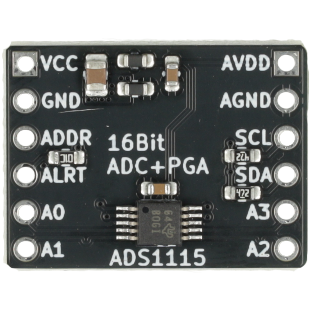
J1 carries VCC, GND, ADDR, ALRT, A0 and A1. J2 carries AVDD, AGND, SCL, SDA, A3 and A2. Both connectors use 2.54 mm pitch. The PCB labels A0-A3 correspond to the IC inputs AIN0-AIN3; ALRT corresponds to ALERT/RDY.
VCC reaches the ADC supply AVDD through ferrite bead FB1. GND reaches the ADC ground AGND through ferrite bead FB2. C1 is 10 µF across VCC/GND, while C2 and C3 are each 100 nF across AVDD/AGND. R1 and R2 provide 4.7 kΩ pull-ups on SCL and SDA; R3 provides a 10 kΩ pull-up on ALRT. All three pull-ups connect to VCC.
The board has no voltage regulator, logic-level converter, external analog input clamps or reverse-polarity protection. AVDD/AGND and VCC/GND are connected through ferrite beads and are not galvanically isolated.
¶ Module views
| Top view | Bottom view | Module and pin headers |
|---|---|---|
 |
 |
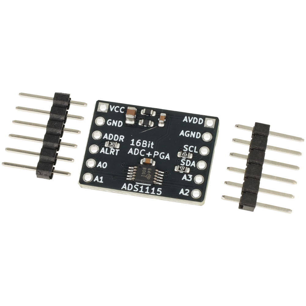 |
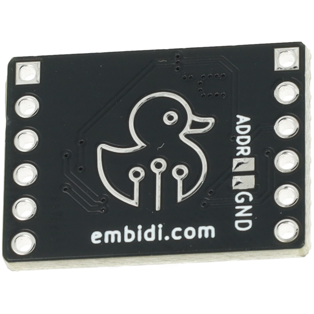
The photographs show the physical module and separate, unsoldered pin headers. The ADDR-GND solder jumper is on the bottom of the board.
¶ Key features
- ADS1115IDGSR 16-bit ADC with four multiplexed analog inputs,
- four single-ended channels, two differential pairs, and additional differential selections supported by the IC,
- selectable full-scale ranges from ±0.256 V to ±6.144 V,
- programmable conversion rates from 8 to 860 SPS,
- I²C addresses 0x48-0x4B selected by the ADDR connection,
- ALRT output for comparator or conversion-ready signalling when configured in software,
- supply and ground ferrite filtering, decoupling capacitors and onboard I²C pull-ups.
¶ Typical applications
- Reading analog voltage-output sensors,
- monitoring low-voltage signals and slow-changing measurements,
- adding analog inputs to an ESP32 or STM32 project,
- evaluating single-ended and differential ADC measurements.
Use suitable external conditioning for signals outside the input range, high source impedances or signals requiring protection or anti-alias filtering.
¶ Specifications
| Parameter | Value | Notes |
|---|---|---|
| IC | ADS1115IDGSR | Texas Instruments, DGS / VSSOP-10 |
| Supply operating range | 2.0-5.5 V | IC voltage is AVDD relative to AGND; no onboard regulator |
| Recommended supply for these examples | 3.3 V at J1.1 VCC | Keeps onboard pull-ups compatible with the shown hosts |
| Resolution | 16 bits, signed output | Single-ended positive readings nominally use codes 0-32767; resolution is not an accuracy guarantee |
| Single-ended inputs | A0, A1, A2, A3 | Measured relative to AGND, one selected channel at a time |
| Differential selections | A0-A1, A0-A3, A1-A3, A2-A3 | Each input must remain within the supply rails |
| Recommended absolute analog input voltage | AGND to AVDD | Independent of the selected full-scale range |
| Conversion rates | 8, 16, 32, 64, 128, 250, 475, 860 SPS | One converter shared between channels; not 860 SPS per channel simultaneously |
| I²C | Standard mode / Fast mode | 100 / 400 kHz; achievable speed depends on bus capacitance and pull-ups |
| I²C addresses | 0x48, 0x49, 0x4A, 0x4B | 7-bit values; ADDR must be connected |
| SDA/SCL pull-ups | 4.7 kΩ each | R2 / R1 to VCC |
| ALRT output | Open-drain, 10 kΩ pull-up to VCC | R3; comparator or conversion-ready function requires configuration |
| IC supply current | 150 µA typical operating; 0.5 µA typical power-down at 25 °C | IC figures; module current also includes pull-up currents and external loads |
| IC temperature rating | -40 to +125 °C | Device rating; the assembled module has no separate environmental qualification stated |
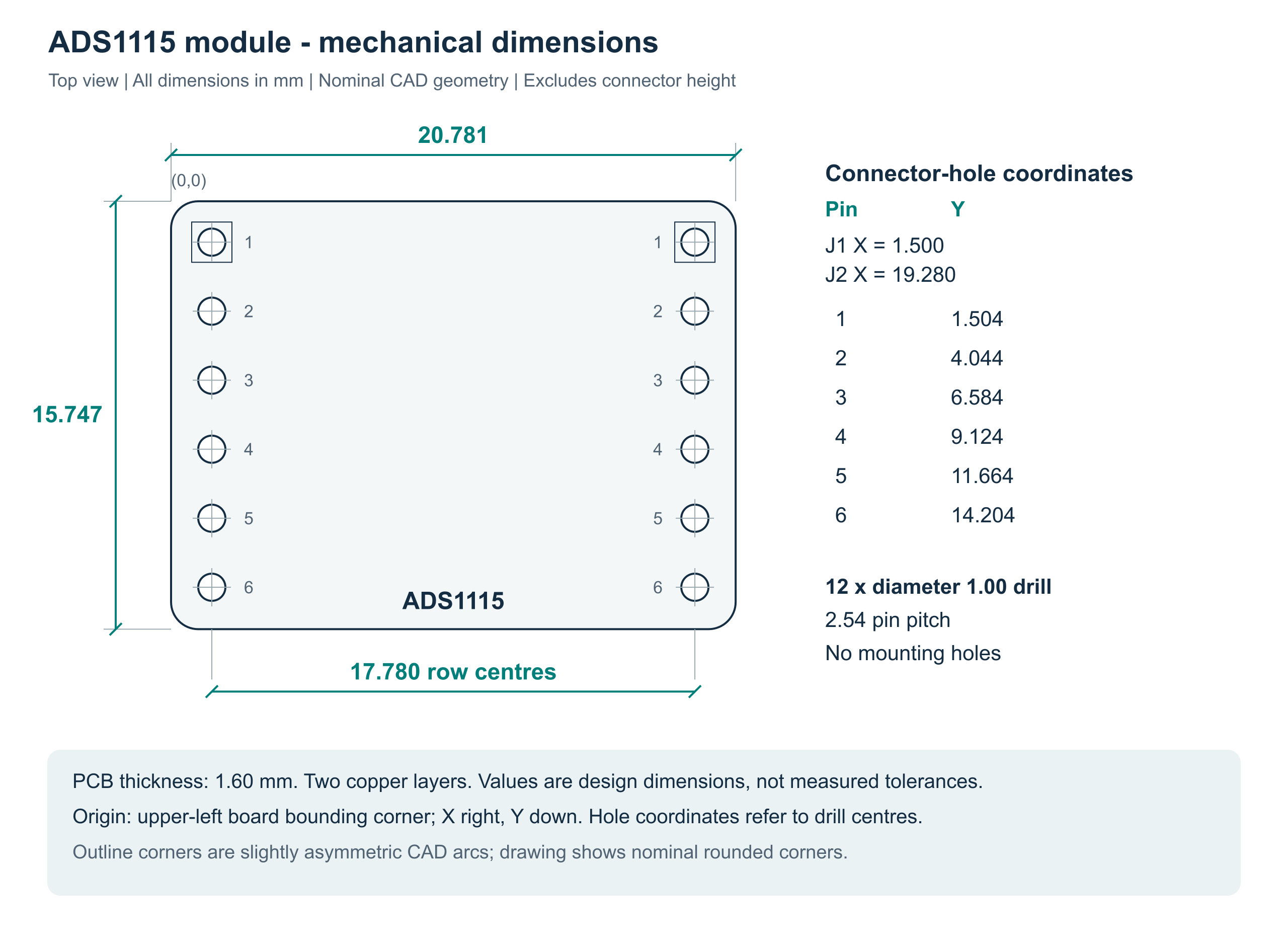
| Headers | 2 × 1×6, 2.54 mm pitch | 17.780 mm between row centres |
| PCB dimensions | 20.781 × 15.747 mm | Outline bounding size from the KiCad board, excluding connectors |
| PCB thickness | 1.60 mm | Project setting; two copper layers |
IC limits and operating conditions are given in the Texas Instruments datasheet, Rev. E, particularly Sections 5, 7 and 8.
¶ Full-scale range and conversion scale
| PGA bits [11:9] | Selected bipolar full-scale range | Voltage per count |
|---|---|---|
000 |
±6.144 V | 187.5 µV |
001 |
±4.096 V | 125 µV |
010 (reset) |
±2.048 V | 62.5 µV |
011 |
±1.024 V | 31.25 µV |
100 |
±0.512 V | 15.625 µV |
101, 110 or 111 |
±0.256 V | 7.8125 µV |
Voltage is the signed conversion result multiplied by the selected voltage-per-count value. Both supplied examples select ±4.096 V, giving 125 µV per count. At a 3.3 V supply, the valid analog voltage is still only AGND to AVDD; the positive full-scale code cannot be reached at this gain. A negative differential result is possible when the selected positive input is below the negative input, while both pins remain within the supply rails.
¶ Pinout
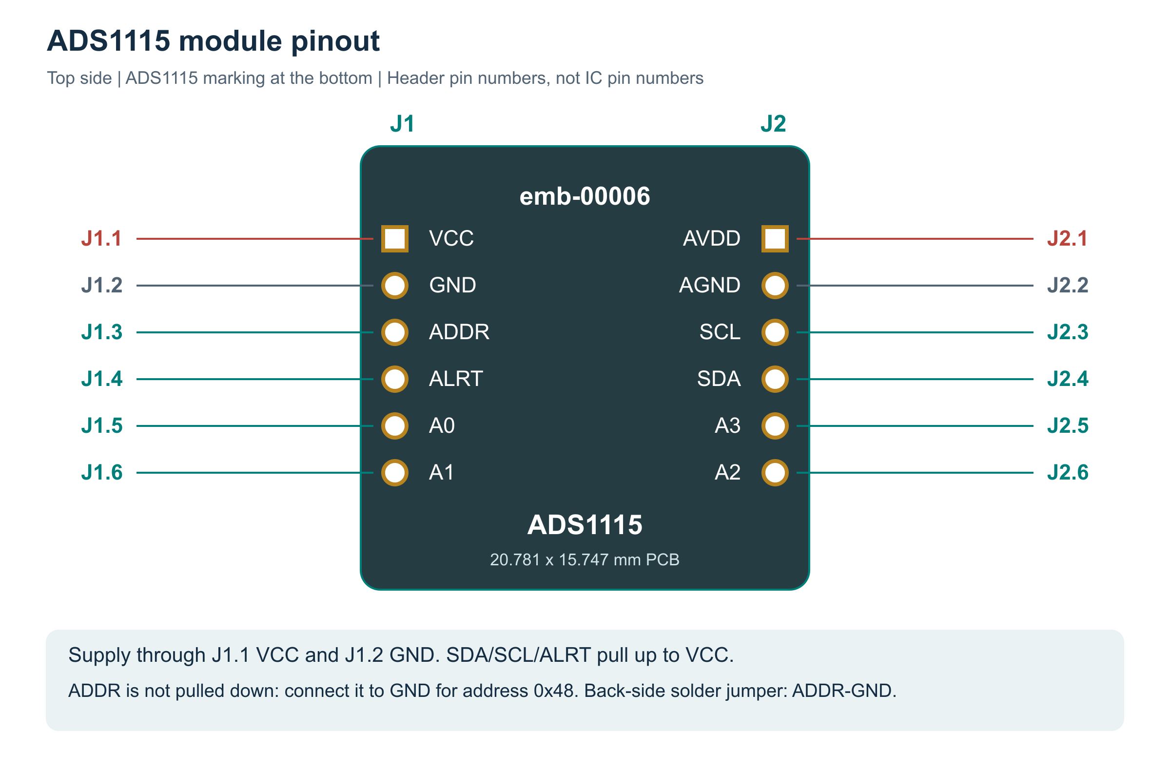
View the board from the component side, with the ADS1115 marking at the bottom. J1 is on the left and J2 is on the right. Pin 1 is the square pad at the top of each row. The numbers below are connector pin numbers, not the IC package pin numbers.
¶ J1 - supply, address and A0/A1
| Pin | PCB label | Type / direction | Function |
|---|---|---|---|
| 1 | VCC | Power input | Main module supply; feeds AVDD through FB1 and supplies the pull-up resistors |
| 2 | GND | Power / return | Main supply and host ground; connected to AGND through FB2 |
| 3 | ADDR | Digital input | I²C address selection; no onboard bias resistor |
| 4 | ALRT | Digital output, open-drain | IC ALERT/RDY output; 10 kΩ pull-up to VCC |
| 5 | A0 | Analog input | IC AIN0 |
| 6 | A1 | Analog input | IC AIN1 |
¶ J2 - filtered rails, I²C and A3/A2
| Pin | PCB label | Type / direction | Function |
|---|---|---|---|
| 1 | AVDD | Filtered power node | ADC VDD after FB1; not a separately regulated output |
| 2 | AGND | Analog reference / return | ADC GND after FB2; reference for A0-A3 |
| 3 | SCL | Digital input | I²C clock; 4.7 kΩ pull-up to VCC |
| 4 | SDA | Digital, bidirectional | I²C data; 4.7 kΩ pull-up to VCC |
| 5 | A3 | Analog input | IC AIN3 |
| 6 | A2 | Analog input | IC AIN2 |
Directions are relative to the module. In the wiring shown below, supply the board through VCC/GND and leave AVDD unconnected externally. Do not connect independent supplies to VCC and AVDD: FB1 connects these nodes. The board is not specified as an auxiliary supply for external loads.
¶ I²C address selection
| ADDR connection | 7-bit address | Module connection |
|---|---|---|
| GND | 0x48 | J1.3 to J1.2, or close the bottom ADDR-GND jumper |
| IC VDD | 0x49 | J1.3 to J2.1 AVDD; bottom jumper open |
| SDA | 0x4A | J1.3 to J2.4; bottom jumper open |
| SCL | 0x4B | J1.3 to J2.3; bottom jumper open |
The KiCad footprint defines the bottom jumper as open. The project has no ADDR pull-down, so 0x48 must not be assumed while ADDR is floating. Check the actual board before wiring it. Both downloaded projects use 0x48. Open the jumper before selecting another address; otherwise it grounds the selected signal or supply. For the SDA address option, also follow the timing requirement in datasheet Section 7.5.1.1.
¶ Connection
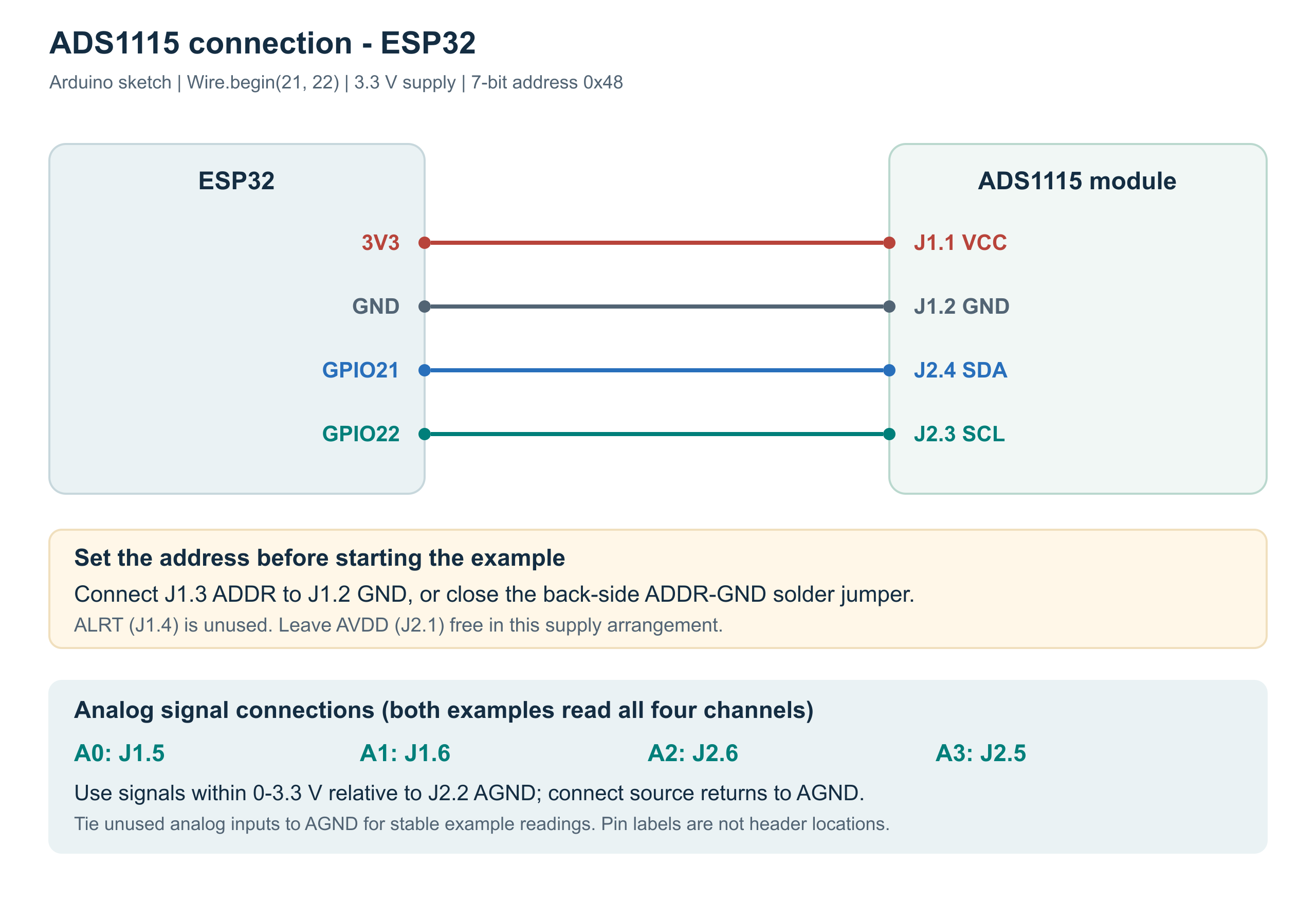
¶ Connections used by the supplied examples
| Module connection | ESP32 Arduino example | NUCLEO-H533RE example |
|---|---|---|
| J1.1 VCC | 3V3 | 3V3 |
| J1.2 GND | GND | GND |
| J2.4 SDA | GPIO21 | PB7 / I2C1_SDA |
| J2.3 SCL | GPIO22 | PB6 / I2C1_SCL |
| J1.3 ADDR | GND, for 0x48 | GND, for 0x48 |
| J1.4 ALRT | Not connected | Not connected |
| J2.1 AVDD | No external connection | No external connection |
| J2.2 AGND | Analog signal-source return | Analog signal-source return |
| A0 / A1 / A2 / A3 | Analog signals within AGND-AVDD | Analog signals within AGND-AVDD |
These assignments come from the supplied .ino, STM32 .ioc and generated I2C initialization. Use the host board's pin labels to locate the pins; the graphics show electrical connections rather than the physical layout of a particular development board.
¶ ESP32
¶ STM32H533
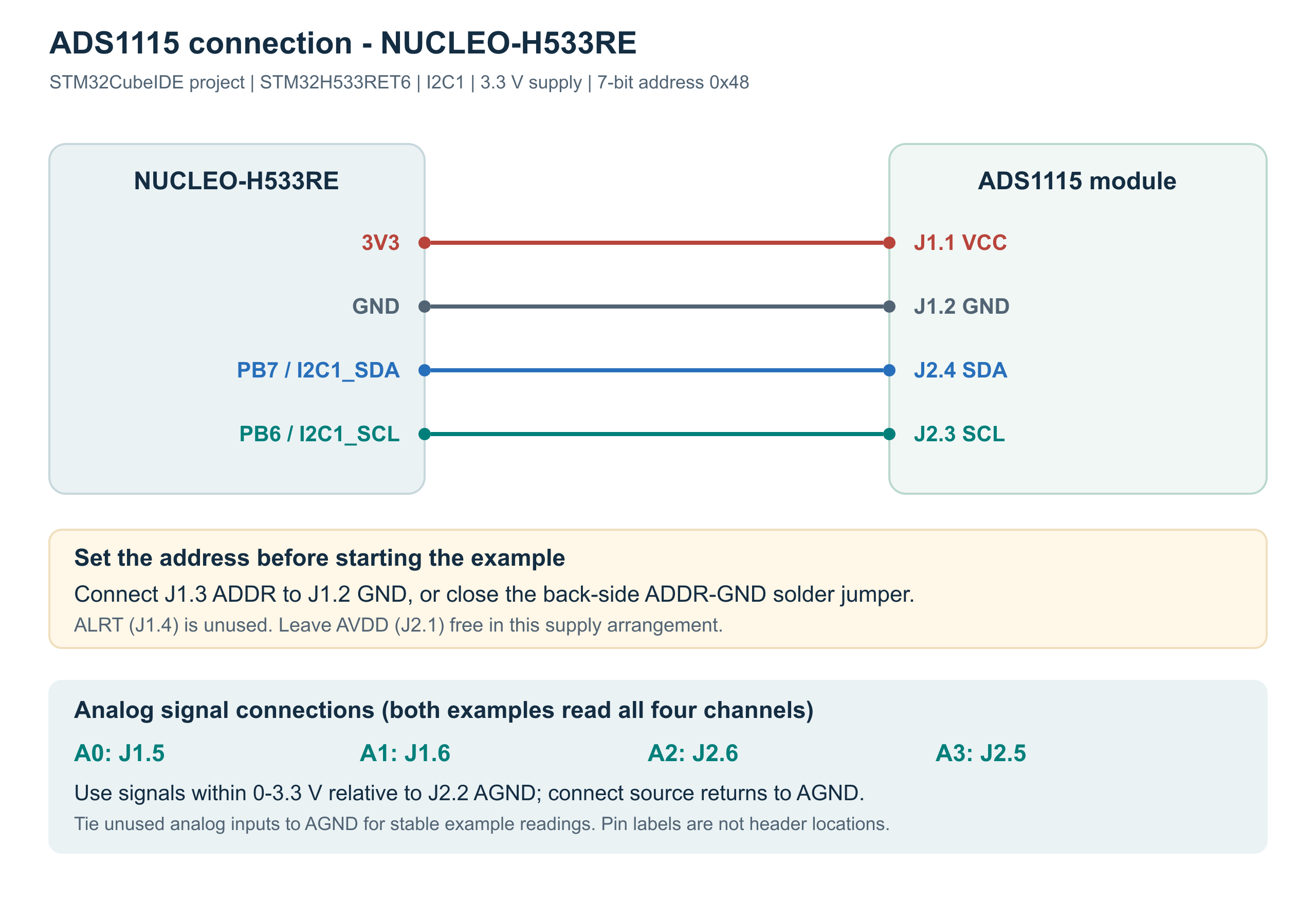
Connect the analog source outputs to A0-A3 and their measurement return to AGND. For the examples, connect unused analog inputs to AGND to obtain stable readings rather than reading floating inputs. Disconnect power before changing the wiring or soldering the address jumper.
¶ Important information and limitations
- Input range: every analog pin must stay between AGND and AVDD during normal operation. The IC absolute-maximum limits of AGND - 0.3 V and AVDD + 0.3 V are stress limits, not a usable measurement range. A ±6.144 V gain setting does not make the module accept ±6.144 V relative to ground.
- Logic voltage: SDA, SCL and ALRT are pulled up to VCC. Powering VCC from 5 V also pulls these lines towards 5 V. Use 3.3 V for the shown ESP32 and STM32 examples; use appropriate level conversion when the host and module use incompatible levels. The IC's minimum input-high level is 0.7 × VDD, so a 5 V-powered IC does not guarantee recognition of a 3.3 V high level.
- Address: the bottom jumper is open in the PCB design and ADDR has no bias resistor. Set the address deliberately before using the examples.
- Ground filtering: AGND and GND are connected through FB2. An additional external short between them bypasses that part of the filtering; these nodes provide no isolation barrier.
- Protection and filtering: the ADC has internal protection structures, but the board adds no external input clamps, input dividers or analog anti-alias filter. Add external conditioning where the application requires it. Do not apply analog signals to an unpowered module.
- Sampling: channels share one converter and are read sequentially. Noise, source impedance, gain, conversion rate, wiring and grounding affect usable accuracy. A nominal 16-bit result does not establish 16-bit system accuracy.
- Multiple boards: their onboard pull-ups appear in parallel. Check the combined pull-up resistance and bus rise time before connecting several modules.
¶ Register reference
For direct I²C access, the main registers are Conversion for the result and Config for setup and conversion status. The addresses below are register pointer values, separate from the module's 7-bit I²C address (0x48 with ADDR connected to GND).
¶ Register map and byte order
| Register pointer | Access | Reset value | Purpose |
|---|---|---|---|
0x00 - Conversion |
Read only | 0x0000 |
Latest completed measurement; signed 16-bit two's complement |
0x01 - Config |
Read / write | 0x8583 |
Start a measurement, check completion and select channel, range, rate and comparator settings |
0x02 - Lo_thresh |
Read / write | 0x8000 |
Lower comparator threshold, in signed ADC counts |
0x03 - Hi_thresh |
Read / write | 0x7FFF |
Upper comparator threshold, in signed ADC counts |
Each register is 16 bits, transferred most-significant byte first. To write, send the pointer byte followed by the high and low data bytes. To read, write the pointer byte, then read two bytes from the same I²C device; a repeated START can join these transactions. Pointer bits 7:2 must be zero. Reading Conversion does not start a new measurement; before the first completed conversion it returns zero.
¶ Config register - 0x01
Binary values in the tables describe the field itself, before shifting it to the indicated bit positions.
| Bits | Field | Meaning |
|---|---|---|
| 15 | OS | Write 1 to start a single-shot conversion while idle; writing 0 has no effect. Read 0 = converting, 1 = idle / single-shot complete. A start request during a conversion has no effect. |
| 14:12 | MUX | Input selection; see the channel table below |
| 11:9 | PGA | Full-scale range and volts per count; see Full-scale range and conversion scale |
| 8 | MODE | 0 = continuous conversions; 1 = single-shot, with power-down between measurements |
| 7:5 | DR | Conversion rate; see the rate table below |
| 4 | COMP_MODE | 0 = traditional threshold comparator; 1 = window comparator |
| 3 | COMP_POL | ALRT polarity: 0 = active low; 1 = active high |
| 2 | COMP_LAT | 0 = nonlatching comparator; 1 = latched until a Conversion read or SMBus alert response |
| 1:0 | COMP_QUE | 00 / 01 / 10 = assert after 1 / 2 / 4 qualifying conversions; 11 = comparator disabled and ALRT high impedance |
After reset, 0x8583 selects A0-A1 differential, ±2.048 V, 128 SPS, single-shot mode and a disabled comparator. No conversion starts automatically in this state. With the comparator disabled, the module's pull-up holds ALRT high. Lo_thresh and Hi_thresh need no changes for the polling sequence below; if using the comparator, recalculate thresholds when changing PGA.
¶ Channel selection - MUX bits [14:12]
| MUX | Measured voltage |
|---|---|
000 |
A0 minus A1 (reset) |
001 |
A0 minus A3 |
010 |
A1 minus A3 |
011 |
A2 minus A3 |
100 |
A0 relative to AGND |
101 |
A1 relative to AGND |
110 |
A2 relative to AGND |
111 |
A3 relative to AGND |
¶ Conversion rate - DR bits [7:5]
| DR | Rate | Nominal conversion time, 1 / rate |
|---|---|---|
000 |
8 SPS | 125 ms |
001 |
16 SPS | 62.5 ms |
010 |
32 SPS | 31.25 ms |
011 |
64 SPS | 15.625 ms |
100 |
128 SPS (reset) | 7.8125 ms |
101 |
250 SPS | 4 ms |
110 |
475 SPS | 2.105 ms |
111 |
860 SPS | 1.163 ms |
These times exclude startup and I²C transfers; the specified data rate can vary by ±10%. Poll OS for single-shot completion with a timeout appropriate to the selected rate. The supplied STM32 example waits 10 ms at 128 SPS; a fixed 10 ms delay would be too short for the lower rates.
¶ Single-shot read sequence
For ±4.096 V, 128 SPS, single-ended inputs and a disabled comparator, write the following configuration to register 0x01. These settings match the supplied STM32 example.
| Channel | Config word, including OS = 1 | I²C data bytes: pointer, high, low |
|---|---|---|
| A0 relative to AGND | 0xC383 |
01 C3 83 |
| A1 relative to AGND | 0xD383 |
01 D3 83 |
| A2 relative to AGND | 0xE383 |
01 E3 83 |
| A3 relative to AGND | 0xF383 |
01 F3 83 |
- With the ADC idle, send the selected three data bytes to I²C address 0x48. For A0, send
01 C3 83. - Select Config by writing pointer
0x01, then read two bytes. Repeat until bit 15 is1; while it is0, the new result is not ready. Stop and report a fault on an I²C error or timeout. - Select Conversion by writing pointer
0x00, then read two bytes, high byte first. Combine them asword = high_byte × 256 + low_byte. - Interpret the word as signed: if it is at least
0x8000, subtract 65536. At this PGA setting, voltage = signed result × 0.000125 V. For example,0x1F40= 8000 counts = 1.000 V, while0xFFFF= -1 count = -0.000125 V. - Repeat from step 1 for the next channel, waiting for each conversion before starting another.
Every analog input must still remain between AGND and AVDD. A negative differential reading describes the difference between two valid input voltages; it does not permit a pin voltage below AGND.
Source: Texas Instruments ADS111x datasheet, Rev. E, Sections 7.5.3-7.5.4 and 8.1, pages 21-27. Configuration words and voltage examples above are calculated from those fields; they have not been tested on hardware as part of this update.
¶ Software
The examples below are the complete supplied archives. Their contents have been preserved. The pin assignments and behaviours were checked from the source and configuration files; compilation and operation on physical hardware have not been verified as part of this documentation.
| Platform | Environment / interface | Download |
|---|---|---|
| ESP32 | Arduino, Wire, Adafruit ADS1X15 | Complete ESP32 sketch |
| NUCLEO-H533RE / STM32H533RET6 | STM32CubeIDE, STM32 HAL, I2C1 | Complete STM32 project |
¶ ESP32 example
The sketch configures SDA on GPIO21, SCL on GPIO22, address 0x48 and GAIN_ONE / ±4.096 V. It reads A0-A3 in single-ended mode, prints the four signed raw values to the serial monitor at 115200 baud, then waits 1000 ms. It does not convert the readings to volts. The conversion data rate is not explicitly set by the sketch and therefore depends on the installed library's default.
- Extract the archive and open
ESP32_ADS1115_EXAMPLE.inoin Arduino IDE with ESP32 board support installed. - Install Adafruit ADS1X15 and its Adafruit BusIO dependency using the library manager. The archive does not bundle or pin these library versions. See the library maintained by Adafruit.
- Wire the module as shown, including the ADDR-to-GND connection, select the correct board and port, and upload the sketch.
- Open the serial monitor at 115200 baud. If initialization cannot find the ADC, the sketch prints an error and stops in a loop.
Download the original ESP32 example
¶ STM32H533 example
The archive targets NUCLEO-H533RE, with STM32H533RET6, I2C1, PB6 SCL, PB7 SDA, and GPIO alternate function AF4. The address is stored in the HAL form 0x48 shifted left by one bit. The .ioc file and generated initialization contain the I²C timing configuration; the 250 MHz I2C1 kernel clock listed in CubeMX is not the SCL bus speed.
The application selects ±4.096 V and 128 SPS in single-shot mode, with a 10 ms wait per conversion. Each loop reads four raw values into raw0-raw3, then performs four new conversions to calculate v0-v3 in volts using 0.000125 V per count. It then waits 1000 ms. The raw and voltage variables therefore represent different conversion instants.
- Extract the entire archive and import
ADS1115_EXAMPLEas an existing STM32CubeIDE project. The archive includes the.ioc, IDE files, HAL/CMSIS sources and application files. - Connect the module as shown and connect the NUCLEO board through its ST-LINK debugger.
- Build the Debug configuration and start a debug session. Place a breakpoint at the delay after the channel reads and inspect
raw0-raw3andv0-v3in the current function scope. - Resume execution to take another set of readings.
There is no UART or USB measurement output in this application. Its transfer calls do not check the HAL return status and use HAL_MAX_DELAY; a communication fault can block execution or leave invalid results. Treat this as an introductory polling example and add error handling when adapting it to an application. ALRT is unused and the comparator is disabled.
Download the original STM32H533 example
¶ Troubleshooting
| Symptom | Checks |
|---|---|
| ADC not found at 0x48 | Check 3.3 V at VCC, AVDD relative to AGND, common host GND, SDA/SCL and a real ADDR-to-GND connection. The address pin must not float. |
| Bus stays low or communication is intermittent | Check shorts, swapped lines, solder joints, host pin configuration, wire length and combined pull-ups. Start with a low I²C clock. |
| Readings change on an unconnected channel | The input is floating. Connect a defined source or connect an unused input to AGND for this test. |
| Reading clips below the expected maximum | Check the selected PGA range and actual input voltage. Each input must stay within AGND-AVDD even if a larger full-scale range is configured. |
| Small negative results near zero | Account for offset and noise; single-ended measurements near ground may produce small negative codes. |
| STM32 shows no serial output | The supplied project has no serial output. Inspect the local measurement variables at a breakpoint. |
| STM32 stops updating | Pause the debugger and inspect the current HAL call, wiring and bus state. The original example uses blocking calls without status checks. |
| Measurements are noisier than expected | Check source impedance, sensor return, supply, ground loops and signal routing; try a lower conversion rate. Onboard ferrites do not replace analog input conditioning. |
¶ Mechanical dimensions
¶ Files
| File | Format | Version | Description |
|---|---|---|---|
| ADS1115 datasheet | December 2024 | Texas Instruments ADS111x datasheet, Rev. E | |
| Module schematic | 1.0 | Electrical schematic | |
| Dimension drawing | 1.0 | PCB dimensions | |
| 3D model | STEP | 1.0 | Nominal 3D assembly |