¶ SN65HVD230 CAN Transceiver Module
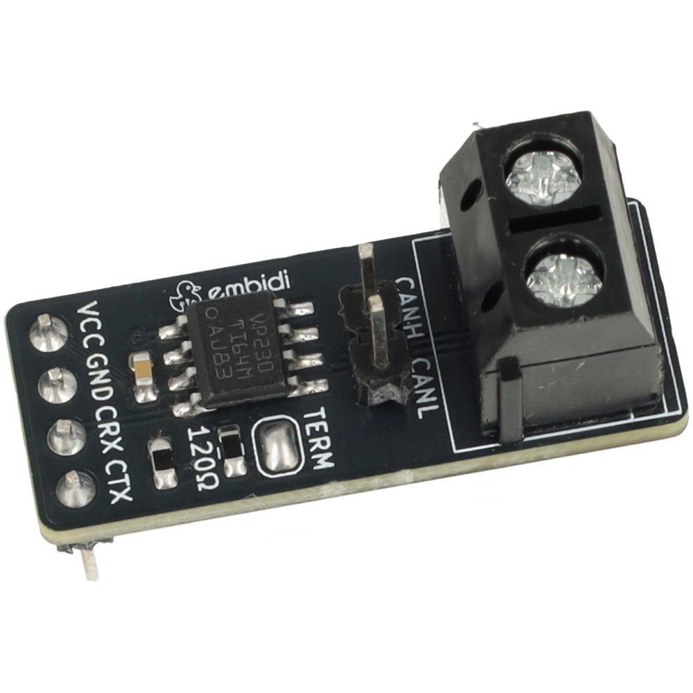
In short: The SN65HVD230 module is a 3.3 V High-Speed CAN physical-layer transceiver. It connects a microcontroller CAN controller to the differential CANH/CANL bus.
Important: The module is not a CAN controller and cannot generate or decode CAN frames by itself. It requires a microcontroller with an integrated CAN controller or an external CAN controller.
| Information | Value |
|---|---|
| Product name | SN65HVD230 CAN Transceiver Module |
| Integrated circuit | SN65HVD230 |
| Module manufacturer | embidi |
| Interface | High-Speed CAN / ISO 11898-2 |
| Supply voltage | 3.0–3.6 V, 3.3 V nominal |
| Logic level | 3.3 V |
| Maximum signaling rate | 1 Mbps |
| PCB revision | 1.0 |
| Last update | 2026-08-13 |
¶ Description
The module provides the physical-layer interface between a CAN controller and a two-wire CAN bus. The transmit signal from the controller is connected to the TXD input, while data received from the bus is passed to the controller through the RXD output. The SN65HVD230 converts 3.3 V logic-level signals into the differential CANH and CANL bus signals.
The module can be used with, among others, ESP32 devices using the TWAI peripheral and STM32 microcontrollers equipped with bxCAN or FDCAN operating in Classical CAN mode. It can also be used with an external CAN controller, provided that its logic levels are compatible with 3.3 V.
The board includes jumpers for enabling the 120 Ω bus termination and selecting one of three operating modes: FAST, SLOPE, or STBY.
¶ Key features
- SN65HVD230 High-Speed CAN transceiver,
- 3.3 V supply and logic levels,
- ISO 11898-2 physical-layer compatibility,
- signaling rate up to 1 Mbps,
- differential CANH and CANL bus lines,
- TXD input and RXD output for connection to a CAN controller,
- selectable 120 Ω bus termination,
- FAST, SLOPE, and STBY modes selected using solder jumpers,
- 10 kΩ resistor for SLOPE mode,
- 100 nF supply decoupling capacitor,
- ESD protection, thermal shutdown, and bus-fault protection integrated in the SN65HVD230.
¶ Typical applications
- CAN communication in STM32 projects,
- TWAI communication with ESP32,
- CAN sensor and actuator nodes,
- embedded-system prototypes,
- CAN bus diagnostics and testing,
- educational projects.
¶ Specifications
| Parameter | Value | Notes |
|---|---|---|
| Integrated circuit | SN65HVD230 | Texas Instruments |
| Module type | High-Speed CAN transceiver | Physical layer |
| Supply voltage | 3.0–3.6 V | 3.3 V nominal |
| Logic level | 3.3 V | TXD, RXD, and RS |
| CAN physical layer | ISO 11898-2 | High-Speed CAN |
| Maximum signaling rate | 1 Mbps | Classical CAN |
| Bus lines | CANH, CANL | Differential pair |
| Logic signals | TXD, RXD | Connection to CAN controller |
| Operating modes | FAST, SLOPE, STBY | Selected using solder jumpers |
| SLOPE resistor | 10 kΩ | RS to GND |
| Bus termination | 120 Ω | Enabled using JP1 |
| Standby current | ~370 µA typical | IC specification |
| Measured current consumption, FAST receiver | 10.41 mA | Measurement performed on the module |
| Measured current consumption, FAST transmitter | 10.46 mA | Measurement performed on the module |
| Measured current consumption, SLOPE transmitter | 8.54 mA | Measurement performed on the module |
| Reference voltage | Approximately VCC / 2 | SN65HVD230 Vref output |
| Bus ESD protection | > ±16 kV HBM | IC specification |
| Number of supported bus nodes | Up to 120 | Based on IC input impedance |
| Operating temperature | -40°C to +85°C | Standard SN65HVD230 device |
| PCB dimensions | 11 x 29 mm | Width x length |
¶ Pinout
| Pin | Type | Direction | Level | Description |
|---|---|---|---|---|
| VCC | Power | Input | 3.3 V | Module supply |
| GND | Power | — | 0 V | Power and signal ground |
| CTX | Digital | Input | 3.3 V logic | Transmit data from the CAN controller |
| CRX | Digital | Output | 3.3 V logic | Receive data to the CAN controller |
| CANH | CAN bus | Bidirectional | Differential signal | CAN High line |
| CANL | CAN bus | Bidirectional | Differential signal | CAN Low line |
¶ TXD and RXD logic
| CAN bus state | TXD | RXD |
|---|---|---|
| Dominant | LOW | LOW |
| Recessive | HIGH | HIGH |
¶ Connection
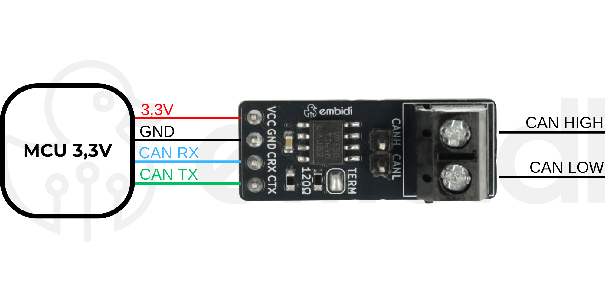
The module requires a regulated 3.3 V supply and a common ground with the CAN controller. Connect the CAN controller transmit output to TXD, the receive input to RXD, and the CANH and CANL lines directly to the corresponding bus wires.
Microcontroller / CAN controller          SN65HVD230 module

3.3 V ----------------------------------> VCC
GND   ----------------------------------> GND
CAN_TX ---------------------------------> CTX
CAN_RX <--------------------------------- CRX

                                           CANH ---- CAN bus CANH
                                           CANL ---- CAN bus CANL
¶ Example connection to common platforms
| Signal | Module pin | ESP32 | STM32 | Notes |
|---|---|---|---|---|
| Supply | VCC | 3.3 V | 3.3 V | Do not use 5 V |
| Ground | GND | GND | GND | Common ground required |
| Transmit | CTX | TWAI TX | CAN_TX / FDCAN_TX | Controller output to transceiver |
| Receive | CRX | TWAI RX | CAN_RX / FDCAN_RX | Transceiver output to controller |
| CAN High | CANH | CAN bus | CAN bus | Connect to CANH |
| CAN Low | CANL | CAN bus | CAN bus | Connect to CANL |
The exact GPIO pins depend on the microcontroller and software configuration.
¶ Module configuration
The module includes four configuration jumpers. JP1 controls the bus termination, while JP2, JP3, and JP4 select the transceiver operating mode.
¶ JP1 – 120R TERM
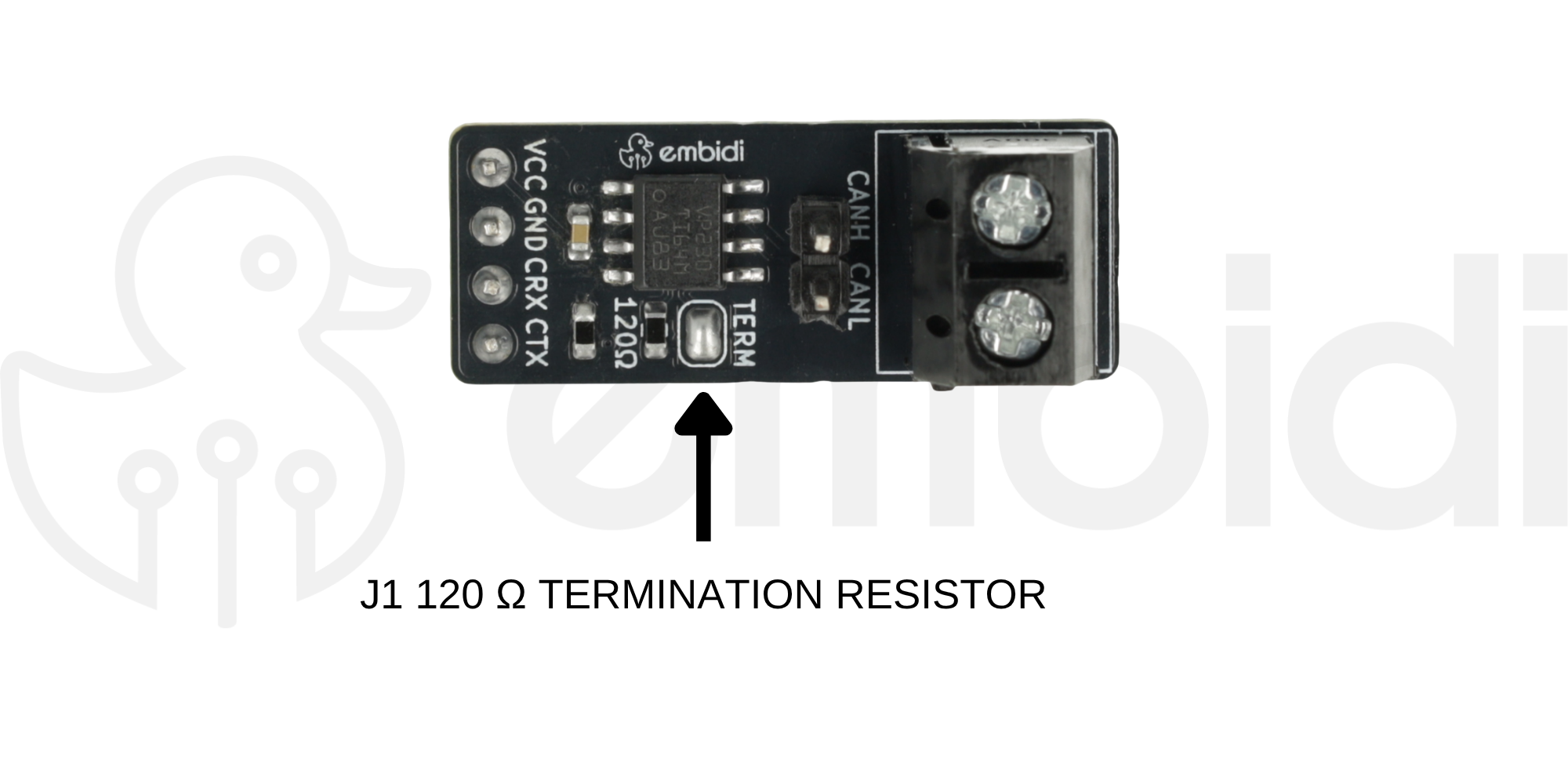
JP1 enables the 120 Ω termination resistor between CANH and CANL.
| JP1 state | Termination |
|---|---|
| Open | 120 Ω resistor disconnected |
| Closed | 120 Ω resistor connected between CANH and CANL |
JP1 should be closed only when the module is located at one of the two physical ends of the main CAN bus.
¶ JP2 – SLOPE
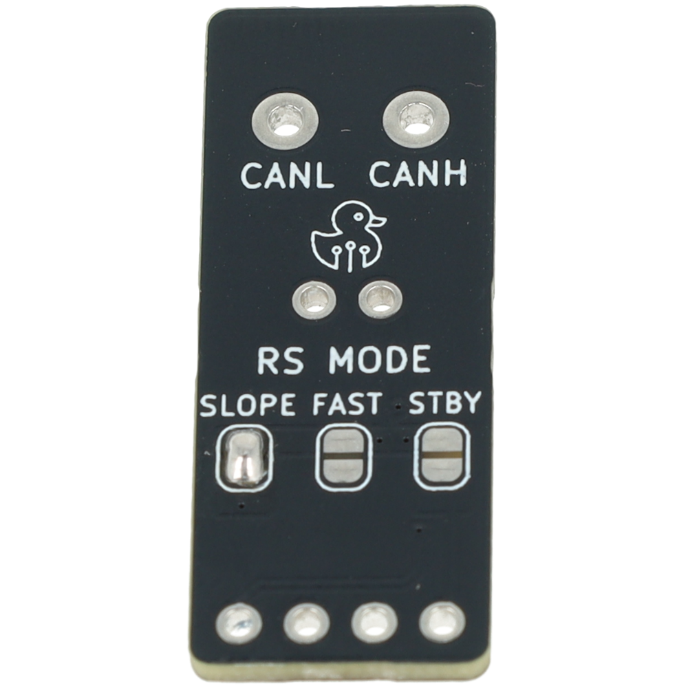
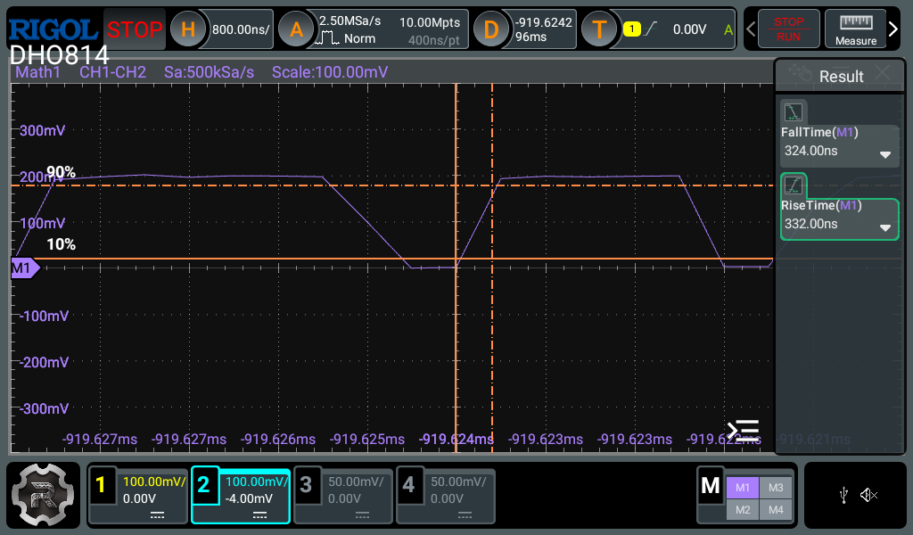
Closing JP2 connects the RS pin of the SN65HVD230 to GND through a 10 kΩ resistor. This limits the output signal transition rate and can reduce overshoot, ringing, and electromagnetic emissions.
The waveform below shows the measured differential CAN signal in SLOPE mode. In this measurement, the rise time between the 10% and 90% levels is approximately 332 ns, while the fall time is approximately 324 ns.
¶ JP3 – FAST
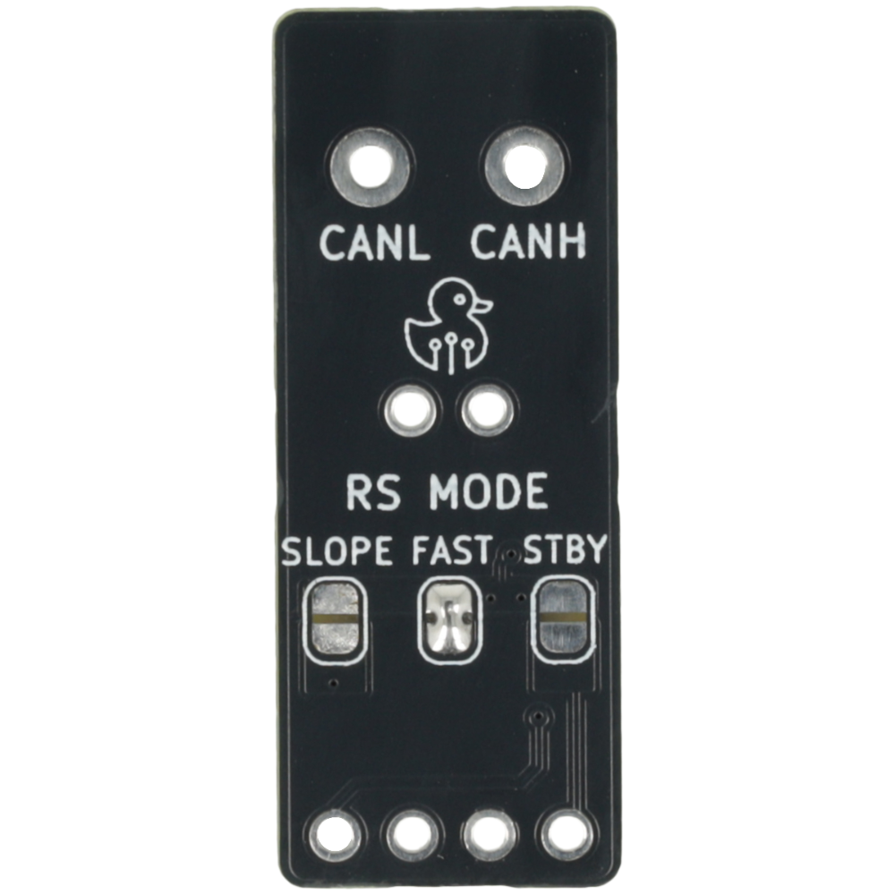
Closing JP3 connects the RS pin directly to GND. The transceiver then operates without intentional slew-rate limiting, providing the fastest CANH and CANL transitions.
The waveform below shows the measured differential CAN signal in FAST mode. In this measurement, the rise time between the 10% and 90% levels is approximately 50 ns, while the fall time is approximately 51 ns.
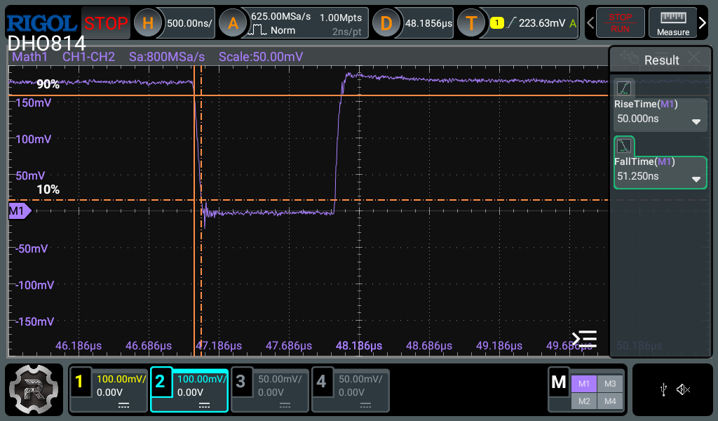
In the performed measurements, the rise time in SLOPE mode was approximately 6.6 times longer than in FAST mode (332 ns compared with 50 ns).
¶ JP4 – STBY
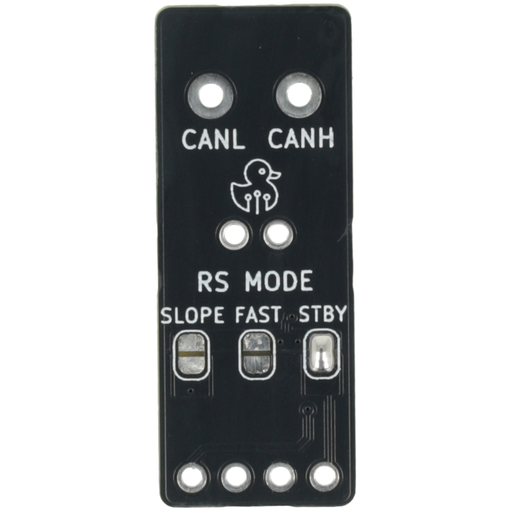
Closing JP4 connects the RS pin to 3.3 V. In Standby mode, the CAN transmitter is disabled and does not actively drive CANH or CANL, while the receiver remains active and can monitor bus activity.
¶ Operating mode summary
| Jumper | Mode | RS connection | Transmitter | Receiver | Typical use |
|---|---|---|---|---|---|
| JP2 | SLOPE | 10 kΩ to GND | Enabled | Enabled | Reduced slew rate |
| JP3 | FAST | Directly to GND | Enabled | Enabled | Maximum speed |
| JP4 | STBY | 3.3 V | Disabled | Enabled | Bus monitoring with lower power consumption |
Important: During normal operation, exactly one of JP2, JP3, or JP4 should be closed.
If none of these jumpers is closed, the RS input is not intentionally configured and this state should not be used as a normal operating mode.
¶ CAN bus termination
A standard CAN bus should use a linear topology with a 120 Ω termination resistor at each of the two physical ends of the main cable.
120 Ω                                              120 Ω
 |                                                   |
CANH ===== Node ===== Node ===== Node ===== Node ===== CANH
CANL ===== Node ===== Node ===== Node ===== Node ===== CANL
If the module is located at one end of the bus, the termination can be enabled using JP1. If the module is located in the middle of the bus, JP1 should remain open.
With the bus powered off, a correctly terminated network containing two 120 Ω resistors should measure approximately 60 Ω between CANH and CANL.
¶ Effect of termination on the signal waveform
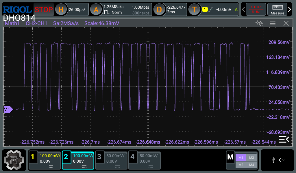
Correct bus termination reduces signal reflections at the ends of the cable and helps maintain a stable differential CAN waveform.
The waveform below shows a correctly terminated bus. Stable signal levels and clear transitions between dominant and recessive states are visible.
For comparison, the waveform below shows the bus without correct termination. Additional pulses and ringing appear after signal transitions as a result of reflections.
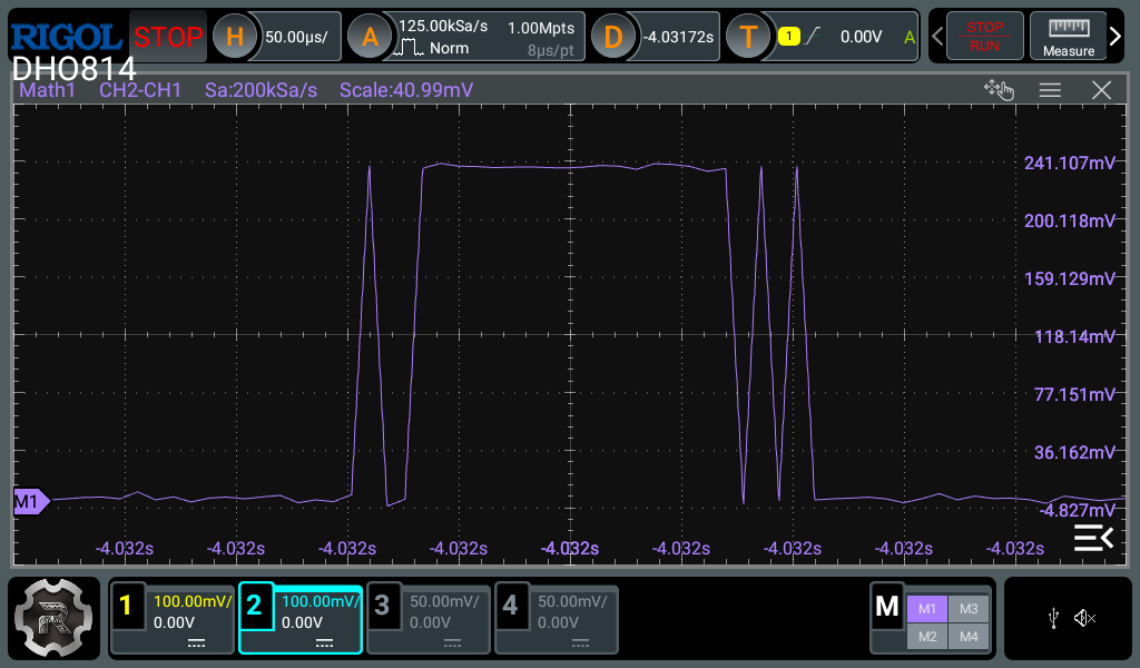
With longer cables or higher signaling rates, these reflections can lead to incorrect interpretation of bus states and unstable communication. Termination should therefore be placed only at the two ends of the main bus, not at every node.
¶ Important information and limitations
- The module should be powered from a regulated 3.3 V supply. Do not apply 5 V directly to VCC.
- The TXD and RS inputs are intended for 3.3 V logic and should not be driven directly by 5 V logic outputs.
- CANH and CANL are differential bus lines and must not be connected to UART, I²C, or other logic-level interfaces.
- TXD and RXD are used to connect the transceiver to a CAN controller and do not form a UART interface.
- Do not close JP3 FAST and JP4 STBY at the same time, because this directly connects 3.3 V to GND through the jumper network.
- The module supports High-Speed Classical CAN up to 1 Mbps.
- The module does not support Low-Speed Fault-Tolerant CAN, Single-Wire CAN, or LIN.
- The STM32 FDCAN peripheral can be used with this module in Classical CAN mode.
- For reliable communication, use twisted-pair wiring for CANH and CANL and keep bus stubs as short as practical.
¶ Oscilloscope verification
To evaluate signal quality, it is best to observe the differential CAN waveform rather than CANH or CANL individually.
Example oscilloscope connection:
CH1 -> CANH
CH2 -> CANL
Probe grounds -> module GND
Then use the oscilloscope math function to display the difference between the two channels, keeping the same polarity when comparing measurements.
In the recessive state, the differential voltage between CANH and CANL should be close to zero. In the dominant state, a positive differential voltage appears between the lines.
When comparing FAST and SLOPE modes, keep the measurement conditions identical: wiring, termination, probes, oscilloscope settings, and CAN signaling rate.
¶ Software
The SN65HVD230 does not require a dedicated software library. Software communicates with the CAN controller integrated into the microcontroller or with an external CAN controller, while the SN65HVD230 implements only the physical layer.
| Platform | CAN peripheral |
|---|---|
| ESP32 | TWAI |
| STM32 | bxCAN or FDCAN in Classical CAN mode |
¶ STM32 example
A ready to use STM32 example is available for the SN65HVD230 module. The project was prepared for the NUCLEO-H533RE board and uses the FDCAN peripheral in Classical CAN mode.
The archive contains two separate projects:
- Transmitter – sends CAN frames through the SN65HVD230 module,
- Receiver – receives CAN frames through the SN65HVD230 module.
Download the STM32 example for SN65HVD230
¶ Files
| File | Format | Version | Description |
|---|---|---|---|
| SN65HVD230 datasheet | April 2018 | Texas Instruments SN65HVD23x datasheet | |
| Module schematic | 1.0 | Electrical schematic | |
| Dimension drawing | 1.0 | PCB dimensions | |
| 3D model | STEP | 1.0 | 3D model |