¶ MCP2562FD CAN / CAN FD transceiver module
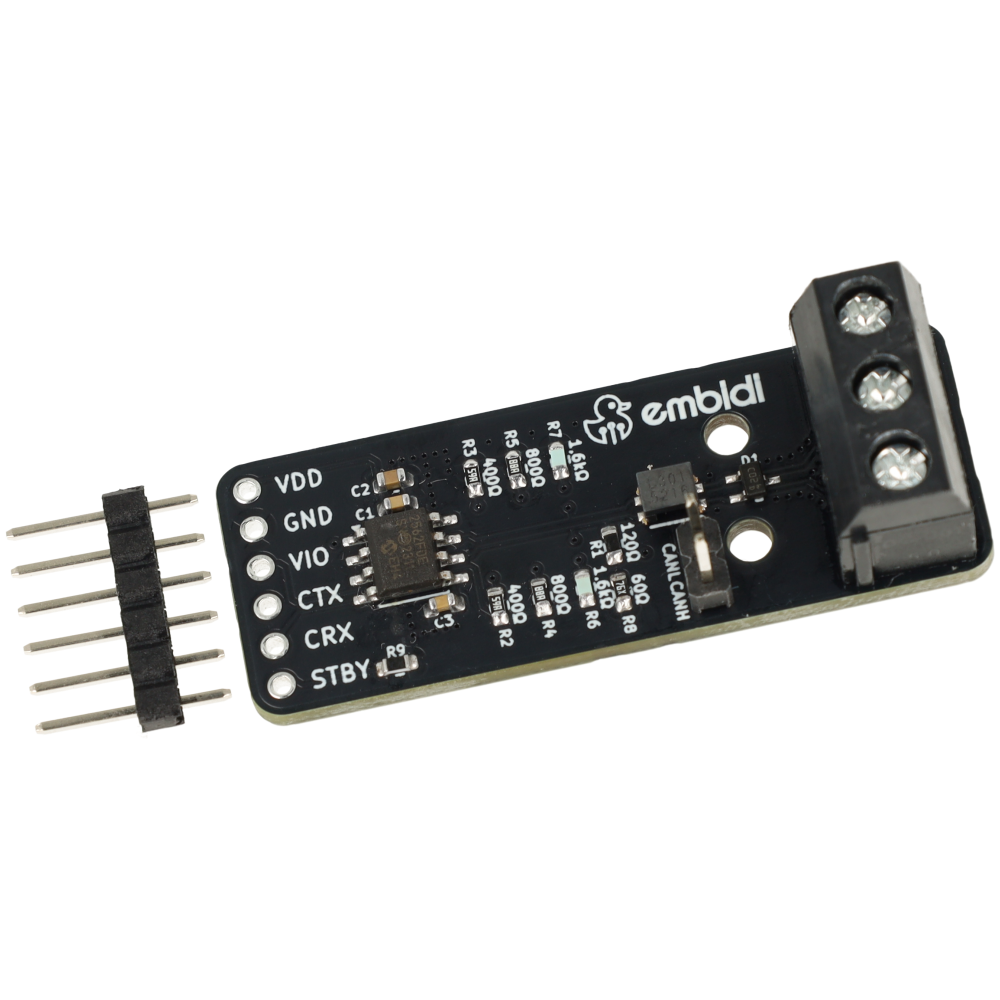
In brief: The MCP2562FD module is a High-Speed CAN / CAN FD physical-layer transceiver. It connects a microcontroller's CAN controller to the differential CANH/CANL bus. It requires a 5 V supply, while the separate VIO input allows the logic levels to match a 3,3 V or 5 V microcontroller.
Important: The module is not a CAN controller and cannot generate or decode CAN frames on its own. It requires a microcontroller with a built-in CAN controller or an external CAN controller. CAN FD communication requires a controller that supports CAN FD.
| Information | Value |
|---|---|
| Product name | MCP2562FD CAN / CAN FD transceiver module |
| Integrated circuit | MCP2562FD-E/SN |
| Module manufacturer | embidi |
| Interface | High-Speed CAN / CAN FD, ISO 11898-2 |
| Transceiver supply | VDD = 5 V |
| Supply and logic levels | VIO = 3,3 V or 5 V |
| Bus termination | 120 Ω, enabled with jumper JP1 |
| Project version | 1.0 |
| Last updated | 2026-09-25 |
¶ Description
The module provides a physical-layer interface between a CAN controller and a two-wire CAN bus. The controller's transmit signal is connected to the CTX input, while data received from the bus is passed to the controller through the CRX output. The CTX and CRX markings on the board correspond to the TXD input and RXD output of the MCP2562FD, respectively.
The transceiver is powered by 5 V supplied to VDD. The separate VIO supply sets the logic levels of the CTX, CRX and STBY signals. This allows the module to work with a 3,3 V microcontroller without changing the bus-side supply.
The module can be used, among other things, with STM32 microcontrollers equipped with CAN or FDCAN and with ESP32 devices equipped with TWAI. The supported frame format depends on the controller's capabilities and configuration — the transceiver itself does not add CAN FD support to a controller that lacks it.
The board includes jumpers for enabling 120 Ω termination and configuring additional line biasing, a common-mode choke and TVS protection. The bus is brought out to a screw terminal and a parallel CANH/CANL pin header.
¶ Key features
- MCP2562FD-E/SN transceiver for High-Speed CAN and CAN FD,
- VDD = 5 V supply and separate VIO = 3,3 V or 5 V logic supply,
- CTX, CRX and STBY signals for connection to a microcontroller,
- jumper-enabled 120 Ω bus termination,
- additional LS-CAN BIAS resistor section,
- ACT1210D-131-2P-TL00 common-mode choke and ESDCAN02-2BWY TVS protection,
- CANL/GND/CANH screw terminal and additional CANH/CANL pin header,
- normal mode by default thanks to a 10 kΩ resistor pulling STBY to GND.
¶ Typical applications
- CAN and CAN FD communication in microcontroller projects,
- bringing up and testing CAN, FDCAN and TWAI peripherals,
- bus diagnostics and monitoring with a suitably configured CAN controller,
- laboratory setups and embedded-system prototypes,
- termination and biasing experiments and bus-signal measurements.
¶ Specifications
| Parameter | Value | Notes |
|---|---|---|
| Integrated circuit | MCP2562FD-E/SN | SOIC-8 package |
| Module type | High-Speed CAN / CAN FD transceiver | Physical layer, without a CAN controller |
| CAN physical layer | ISO 11898-2 | High-Speed CAN |
| Transceiver supply | 5 V | VDD input, external supply |
| Logic supply | 3,3 V or 5 V | VIO input, external supply |
| Logic levels | Determined by VIO | CTX, CRX and STBY |
| Bus lines | CANH, CANL | Differential pair |
| Logic signals | CTX, CRX | Connection to the CAN controller |
| Operating modes | Normal, Standby | Selected with the STBY input |
| STBY resistor | 10 kΩ | R9, connects STBY to GND |
| Bus termination | 120 Ω | R1, enabled with jumper JP1 |
| Bias resistors | 402 Ω, 806 Ω, 1,6 kΩ | Pairs selected with jumpers JP2–JP7 |
| Additional CANL load | 60,4 Ω to GND | R8, enabled with jumper JP8 |
| Common-mode choke | ACT1210D-131-2P-TL00 | L1, 130 µH |
| Bus protection | ESDCAN02-2BWY | D1, TVS / ESD |
| VDD capacitors | 100 nF and 1 µF | C1 and C2 |
| VIO capacitor | 100 nF | C3 |
| Microcontroller connector | 1×6 pin header, 2,54 mm pitch | J1 |
| Bus screw terminal | MKDS 1,5-3-5,08 | J2, 5,08 mm pitch |
| Additional bus connector | 1×2 pin header, 2,54 mm pitch | J3 |
| PCB dimensions | 44,05 × 16,55 mm | Board outline dimensions |
| PCB thickness | 1,6 mm | Two-layer board |
¶ Pinout
¶ J1 — microcontroller connector
A 1×6 pin header with a 2,54 mm pitch. Signal names are marked on the top side of the board. Directions in the table are given relative to the module.
| Pin | Signal | Type | Direction | Level | Description |
|---|---|---|---|---|---|
| 1 | VDD | Power | Input | 5 V | Transceiver supply |
| 2 | GND | Power | — | 0 V | Power and signal ground |
| 3 | VIO | Power | Input | 3,3 V or 5 V | Logic-interface supply |
| 4 | CTX | Digital | Input | VIO logic | Data transmitted from the CAN controller; transceiver TXD input |
| 5 | CRX | Digital | Output | VIO logic | Data received by the CAN controller; transceiver RXD output |
| 6 | STBY | Digital | Input | VIO logic | Operating-mode selection; 10 kΩ resistor to GND |
¶ J2 — bus screw terminal
A three-pin connector with a 5,08 mm pitch. The CANL, GND and CANH markings are on the bottom side of the board.
| Pin | Signal | Type | Direction | Description |
|---|---|---|---|---|
| 1 | CANL | CAN bus | Bidirectional | CAN Low line |
| 2 | GND | Ground | — | Bus reference ground |
| 3 | CANH | CAN bus | Bidirectional | CAN High line |
¶ J3 — additional bus connector
A 1×2 pin header with a 2,54 mm pitch. It is connected in parallel with the bus lines on J2, on the connector side of choke L1.
| Pin | Signal | Type | Direction | Description |
|---|---|---|---|---|
| 1 | CANH | CAN bus | Bidirectional | CAN High line |
| 2 | CANL | CAN bus | Bidirectional | CAN Low line |
J3 can be used to connect measurement probes or an additional node on a test bench. The connector has no ground pin — GND must be taken from J1 or J2.
In the schematic, CAN+ and CAN_OUT+ correspond to CANH, while CAN- and CAN_OUT- correspond to CANL. The CAN_OUT+ and CAN_OUT- nets are on the bus-connector side.
¶ Connection
The module requires VDD = 5 V, a VIO supply matching the microcontroller's logic levels, and a common ground. Connect the CAN controller's transmit output to CTX, its receive input to CRX, and CANH and CANL to the corresponding bus wires.
Example for a microcontroller with 3,3 V logic:
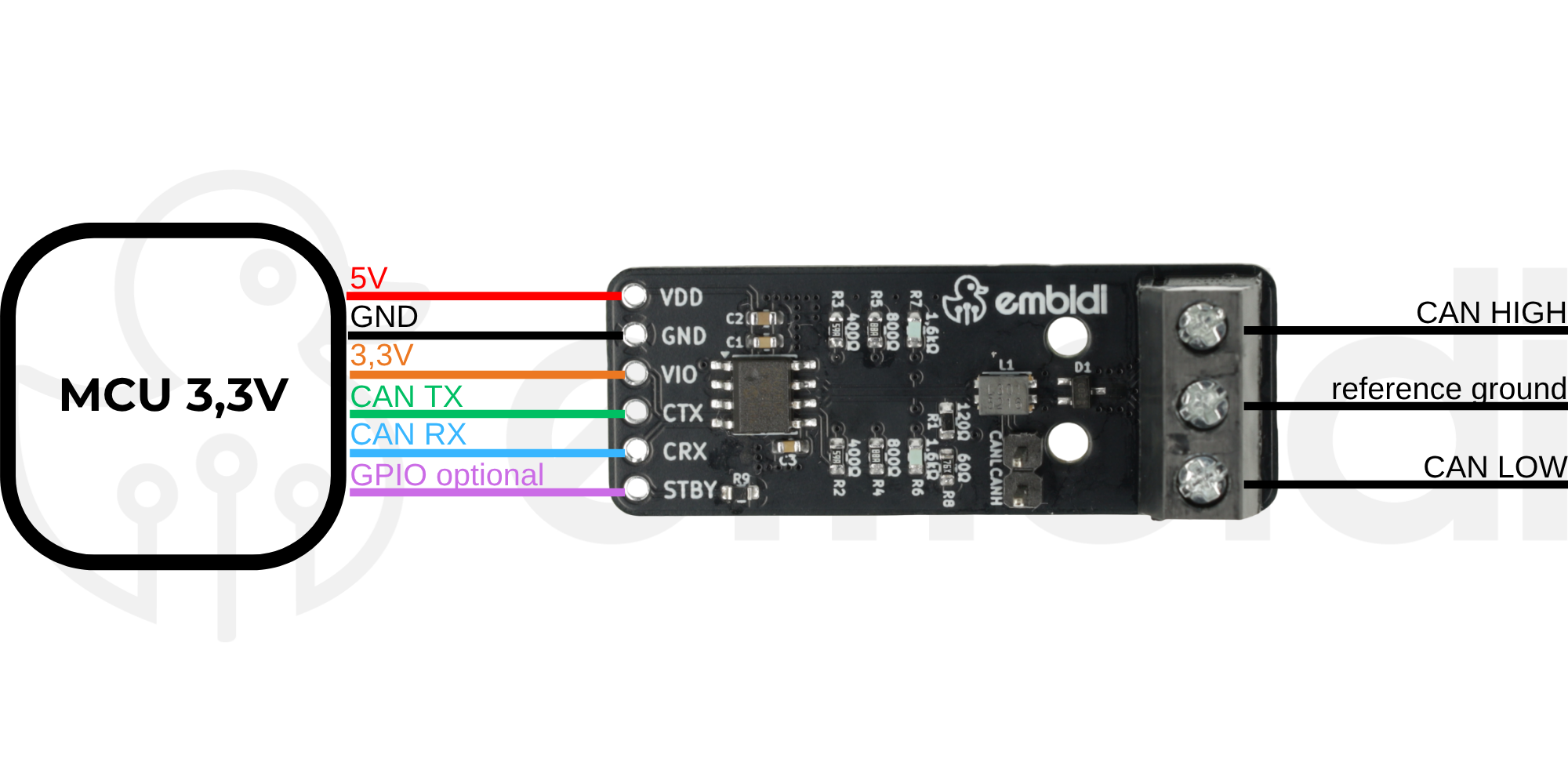
Power supply / microcontroller       MCP2562FD module

5 V --------------------------------> VDD
GND --------------------------------- GND
3,3 V ------------------------------> VIO
CAN_TX -----------------------------> CTX
CAN_RX <----------------------------- CRX
GPIO, optional ---------------------> STBY

                                       CANH ---- bus CANH
                                       CANL ---- bus CANL
                                       GND ----- reference ground
STBY can be left unconnected — resistor R9 then keeps the module in normal mode.
¶ Example connections to popular platforms
The following table applies to microcontrollers operating with 3,3 V logic.
| Signal | Module pin | ESP32 with TWAI | STM32 with CAN / FDCAN | Notes |
|---|---|---|---|---|
| Transceiver supply | VDD | 5 V source | 5 V source | Also required with 3,3 V logic |
| Ground | GND | GND | GND | Common ground |
| Logic supply | VIO | 3,3 V | 3,3 V | Voltage matching the microcontroller's logic |
| Transmit | CTX | TWAI TX | CAN_TX / FDCAN_TX | Controller output to the transceiver |
| Receive | CRX | TWAI RX | CAN_RX / FDCAN_RX | Transceiver output to the controller |
| Operating mode | STBY | GPIO or unconnected | GPIO or unconnected | Low level means normal mode |
| CAN High | CANH | CAN bus | CAN bus | Connection to CANH |
| CAN Low | CANL | CAN bus | CAN bus | Connection to CANL |
The specific GPIO pins depend on the microcontroller and software configuration. CAN FD support depends on the capabilities of the selected controller.
Important: VDD and VIO serve different purposes. With a 3,3 V microcontroller, supply 5 V to VDD and 3,3 V to VIO. Powering VIO alone does not replace the VDD supply.
¶ Module configuration
The module has eight solder jumpers on the bottom side of the board. JP1 enables termination, JP2–JP7 select the bias resistors, and JP8 connects an additional CANL load. All jumpers are open by default. Changing their state requires soldering.
Normal or Standby mode is selected separately using the STBY input on J1.
¶ JP1 — TERM 120Ω / HS ONLY
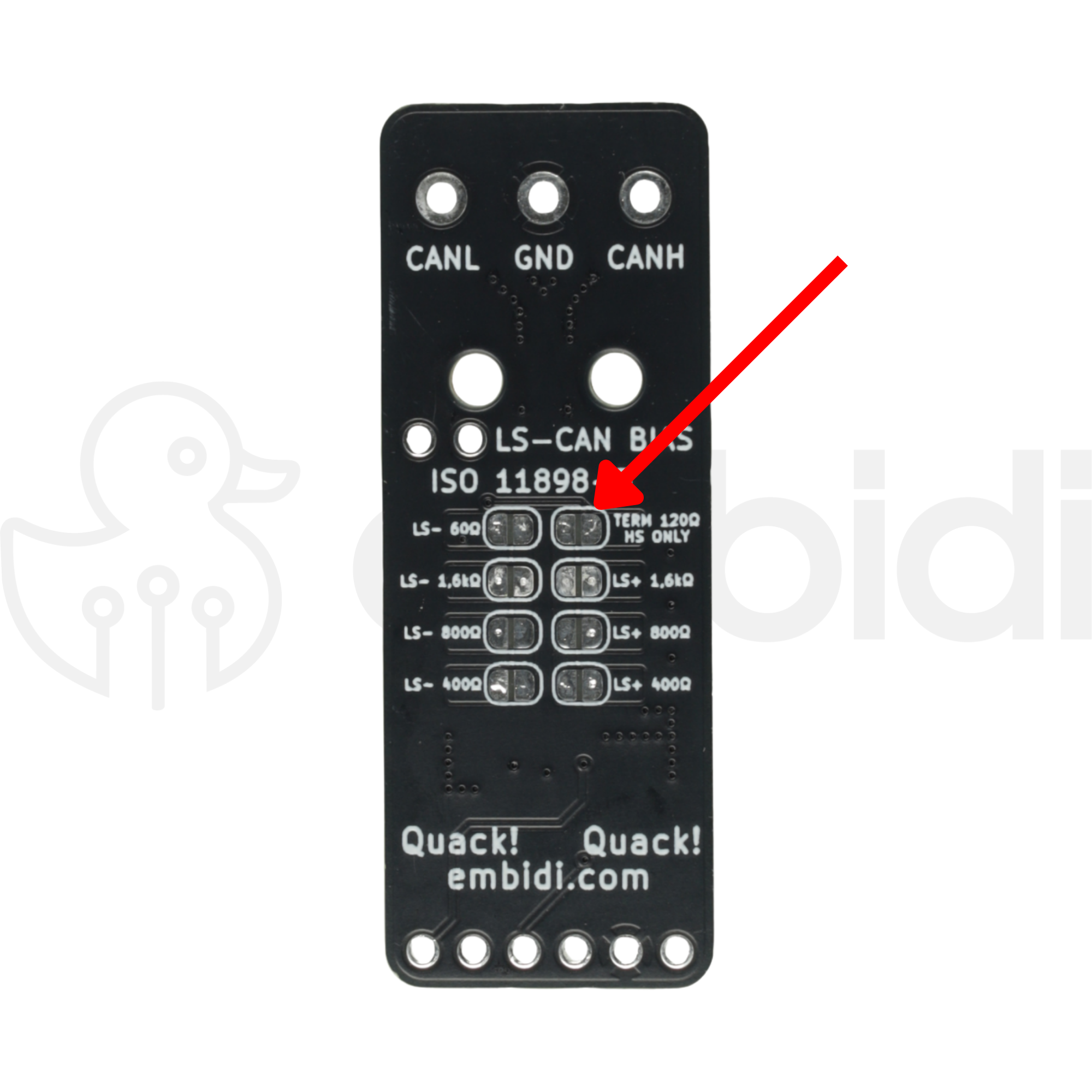
Closing JP1 connects resistor R1 = 120 Ω between CANH and CANL. The resistor is on the transceiver side, before choke L1.
| JP1 state | Termination |
|---|---|
| Open | 120 Ω resistor disconnected |
| Closed | 120 Ω resistor connected between CANH and CANL |
JP1 should be closed only when the module is at one of the two physical ends of the main bus cable and is intended to provide termination there.
¶ JP2–JP7 — LS-CAN BIAS
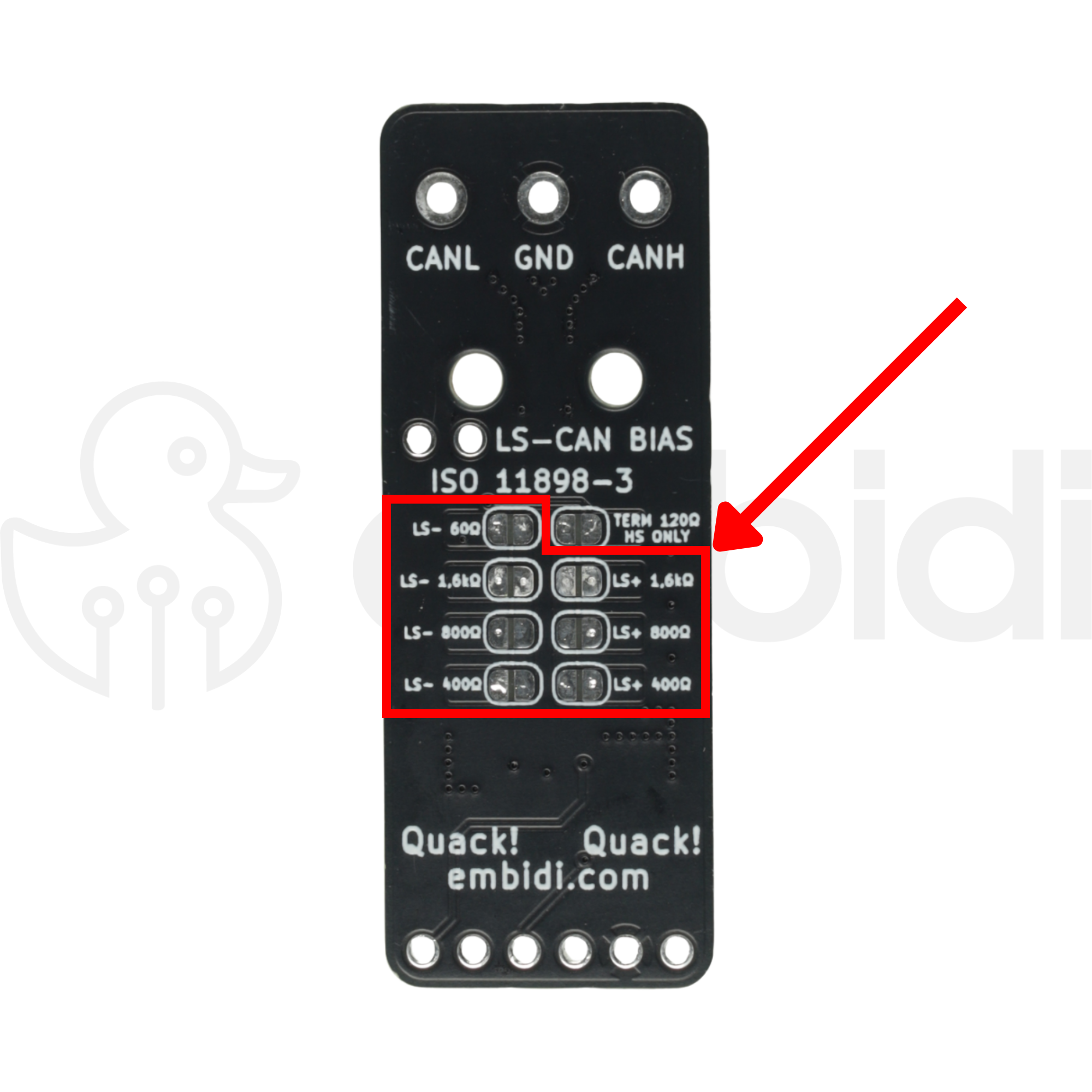
The section marked ISO 11898-3 / LS-CAN BIAS on the board allows CANL to be pulled up to VDD and CANH to be pulled down to GND through selected resistors. It is intended for communication experiments with buses that use this type of biasing.
| Jumper | Resistor | Connection when closed | Board marking |
|---|---|---|---|
| JP2 | R2 = 402 Ω | CANL to VDD | LS- 400Ω |
| JP3 | R3 = 402 Ω | CANH to GND | LS+ 400Ω |
| JP4 | R4 = 806 Ω | CANL to VDD | LS- 800Ω |
| JP5 | R5 = 806 Ω | CANH to GND | LS+ 800Ω |
| JP6 | R6 = 1,6 kΩ | CANL to VDD | LS- 1,6kΩ |
| JP7 | R7 = 1,6 kΩ | CANH to GND | LS+ 1,6kΩ |
The resistors are selected in pairs: one for CANH and the other for CANL.
| Jumper pair | Resistance of each branch | Variant marking in the project |
|---|---|---|
| JP2 + JP3 | 402 Ω | 4 node |
| JP4 + JP5 | 806 Ω | 8 node |
| JP6 + JP7 | 1,6 kΩ | 16 node |
The variants are described in the project by the rule R per node = n × 100 Ω, where n is the number of devices.
Select one jumper pair and leave the other pairs open. In this configuration, JP1 must remain open. The 400 Ω and 800 Ω values printed on the board are rounded; the actual resistor values in the project are 402 Ω and 806 Ω.
Important: The LS-CAN BIAS section changes the resistor network, not the type of transceiver. The MCP2562FD remains a High-Speed CAN transceiver. Closing the jumpers does not provide full Low-Speed Fault-Tolerant CAN functionality under ISO 11898-3, including line-fault detection and single-wire operation after a fault.
For standard HS CAN / CAN FD operation, leave JP2–JP7 open.
¶ JP8 — LS- 60Ω
Closing JP8 connects resistor R8 = 60,4 Ω between CANL and GND. This is a separate, asymmetric option intended for CANL loading experiments, not a 120 Ω termination between CANH and CANL.
| JP8 state | CANL load |
|---|---|
| Open | 60,4 Ω resistor disconnected |
| Closed | 60,4 Ω resistor connected between CANL and GND |
The 60 Ω marking on the board is rounded. JP8 remains open for standard HS CAN / CAN FD communication.
¶ STBY — operating-mode selection
The STBY input is connected to GND through resistor R9 = 10 kΩ. This means the module also starts in normal mode when the STBY pin is left unconnected.
| STBY state | Operating mode | Notes |
|---|---|---|
| Unconnected | Normal | R9 holds the input low |
| Low | Normal | Standard CAN / CAN FD communication |
| High | Standby | High level in the VIO voltage domain |
A microcontroller GPIO output with logic levels matching VIO can be used to control STBY.
¶ Summary of standard configurations
| Application | JP1 | JP2–JP7 | JP8 | STBY |
|---|---|---|---|---|
| Node at the end of the bus, with no other terminator at that location | Closed | Open | Open | Low or unconnected |
| Intermediate node or point with an existing terminator | Open | Open | Open | Low or unconnected |
| Additional sniffer on a correctly terminated HS CAN / CAN FD bus | Open | Open | Open | Low or unconnected |
Leaving the jumpers open does not connect any additional termination or bias resistors. However, it does not replace the CAN controller configuration required for sniffer operation.
¶ CAN bus termination
A standard High-Speed CAN / CAN FD bus should have a linear topology and a 120 Ω resistor at each of the two physical ends of the main cable.
CANH ---+-------------+-------------+-------------+---
        |             |             |             |
       120 Ω        [Node]        [Node]         120 Ω
        |             |             |             |
CANL ---+-------------+-------------+-------------+---
If the module is at the end of the bus, termination can be enabled with JP1. If the module is in the middle of the bus or a terminator is already connected at that location, JP1 should remain open.
With bus power off, two 120 Ω termination resistors give a reading of approximately 60 Ω between CANH and CANL. With one terminator, the reading is approximately 120 Ω. These are indicative values for a standard HS configuration without additional biasing.
¶ Effect of termination on the signal waveform
Correct termination reduces signal reflections at the ends of the cable and helps maintain a stable differential waveform. Missing or incorrectly placed termination can cause oscillations after signal edges and make reliable reception more difficult.
Termination should be placed at the two ends of the main cable, not at every node. Connecting a sniffer to a correctly terminated bus does not require another 120 Ω resistor.
¶ Important information and limitations
- VDD requires a 5 V supply. Choose the VIO voltage to match the controller's logic levels: 3,3 V or 5 V. These are two separate supply rails.
- CTX and CRX connect the transceiver to the CAN controller. They do not form a UART interface and must not be connected directly to the bus wires.
- CANH and CANL are differential bus lines, not microcontroller logic signals.
- CAN FD support requires a suitable controller. Using the MCP2562FD does not extend the capabilities of a Classical CAN controller.
- In a standard HS CAN / CAN FD configuration, JP2–JP8 remain open. JP1 is enabled only to provide termination at the end of the bus.
- Do not combine JP1 termination with an LS-CAN BIAS configuration. The bias section does not provide Low-Speed Fault-Tolerant transceiver functionality.
- J3 has no GND pin. Reference ground must be taken from J1 or J2.
- Use twisted-pair cable for CANH and CANL and keep bus stubs as short as possible.
¶ Oscilloscope verification
To assess signal quality, observe the CANH − CANL differential waveform rather than only the voltage of one line relative to ground.
Example oscilloscope connection:
CH1 -> CANH
CH2 -> CANL
Probe grounds -> module GND

Math function: CH1 - CH2
The J3 connector can be used to connect the channels. Because it has no ground pin, connect the probe grounds to GND on J1 or J2, not to CANH or CANL.
In a standard HS CAN / CAN FD configuration, the differential voltage is close to zero in the recessive state, while a positive differential voltage appears between CANH and CANL in the dominant state.
When comparing configurations, keep the conditions the same: cables, termination, probes, oscilloscope settings and transmission parameters. For CAN FD, account separately for the arbitration-phase and data-phase settings.
The captures below were recorded with a Rigol DHO814 and a NUCLEO-H533RE connected to this MCP2562FD module. The bus operated at 500 kbit/s in CAN FD mode without bit rate switching (BRS). This measurement setup differs from the downloadable STM32 example, which uses BRS.
¶ With bus termination
Termination was present during these captures, but the number of connected terminators was not recorded. The probes were reversed relative to the connection shown above: CH1 measured CANL and CH2 measured CANH. The Math trace therefore uses CH2 − CH1 to show CANH − CANL.
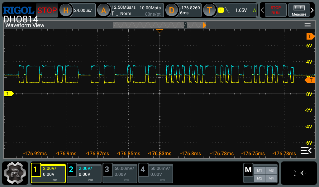
CANH and CANL during part of a CAN FD frame. CH1 (yellow) shows CANL and CH2 (cyan) shows CANH.
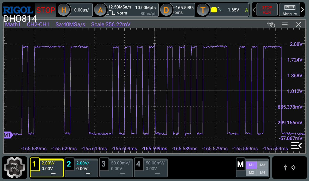
The differential signal shows approximately 2 V in the dominant state and approximately 0 V in the recessive state.
¶ Without bus termination
For these captures, CH1 measured CANH and CH2 measured CANL; the Math trace uses CH1 − CH2. Removing termination changes both the dominant voltage and the return to the recessive state.
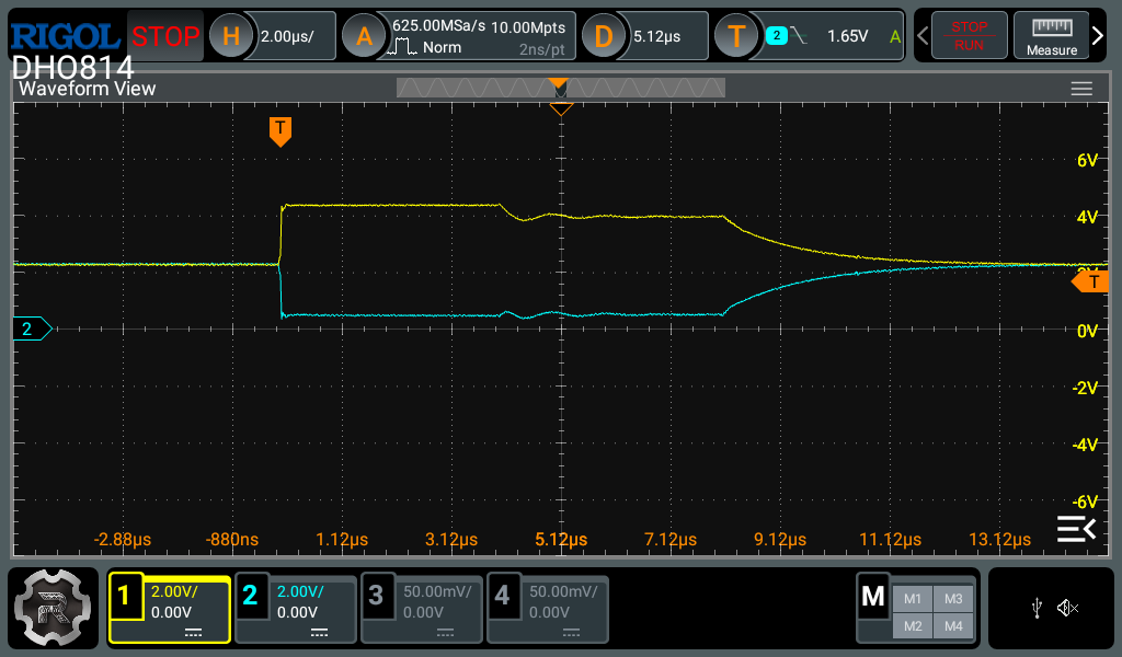
After the dominant interval, both lines return slowly toward their recessive levels.
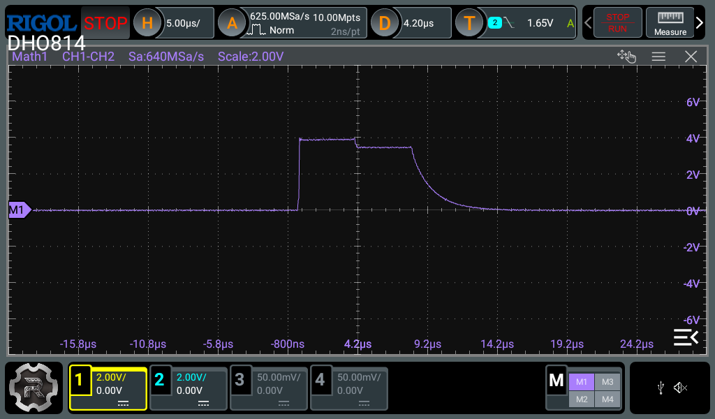
The differential voltage reaches approximately 4 V and then decays over several microseconds after the dominant interval.
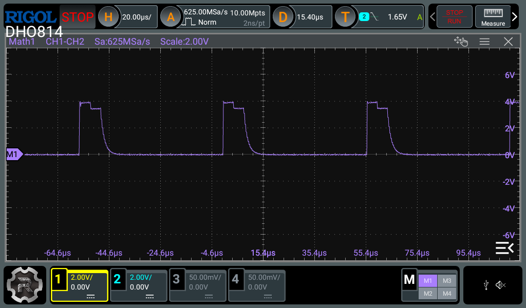
Repeated short differential pulses observed in this setup without termination.
¶ Software
The MCP2562FD does not require a separate software library. The software controls the CAN controller built into the microcontroller or an external CAN controller, while the MCP2562FD implements the physical layer.
| Platform | CAN peripheral | Notes |
|---|---|---|
| ESP32 equipped with TWAI | TWAI | Frame format depends on the capabilities of the selected device |
| STM32 equipped with CAN | CAN / bxCAN | Classical CAN communication |
| STM32 equipped with FDCAN | FDCAN | Classical CAN or CAN FD, depending on configuration |
| Microcontroller with an external CAN controller | Depends on the controller | Logic levels must match VIO |
The transmission speed, frame format and controller operating mode are configured in software. The parameters must match the bus configuration. For CAN FD, the data phase must also be configured.
¶ STM32 example
A ready-to-use STM32 example is available for the MCP2562FD CAN FD module. The projects target the NUCLEO-H533RE board and use its FDCAN peripheral in CAN FD mode with bit rate switching (BRS).
The archive contains two separate projects:
- Transmitter – sends CAN FD frames through the MCP2562FD module,
- Receiver – receives CAN FD frames through the MCP2562FD module.
Download the STM32 example for MCP2562FD
¶ Files
| File | Format | Version | Description |
|---|---|---|---|
| MCP2562FD — manufacturer's page | Website | — | Device documentation on the Microchip website |
| Module schematic | 1.0 | Electrical schematic | |
| Dimension drawing | 1.0 | PCB dimensions | |
| 3D model | STEP | 1.0 | 3D model |